Board Thickness versus Dielectric Thickness in PCB
This example shows how to define the board thickness of a PCB with respect to the dielectric thickness of pcbStack object for different use-cases. This example has three sections for three different use cases as below:
Single-layered dielectric PCB
Multi-layered dielectric PCB
Importing the PCB design using a
pcbReaderobject.
The value of the BoardThickness property of the pcbStack object is the sum of thicknesses of all the dielectric layers that lie below the top metal layer. Dielectric layers above the top metal layer are considered as coating and are not included in the BoardThickness calculations. You must define the BoardThickness before defining the Layers.
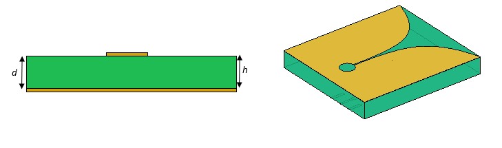
Single-Layered dielectric pcbStack
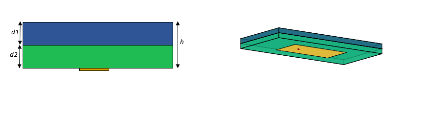
The PCB in this use case has a single dielectric layer sandwiched between the top and bottom metal layers with BoardThickness defined by h and the dielectric Thickness defined by d.
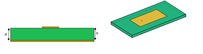
When the pcbStack has a single dielectric layer, the BoardThickness (h) must be equal to the dielectric Thickness (d). Otherwise, d is updated to match h.
p = pcbStack;
sub = dielectric('Fr4');
TopMetal = p.Layers{1};
BtmMetal = p.Layers{2};
p.BoardThickness = sub.Thickness;
p.Layers = {TopMetal,sub,BtmMetal};
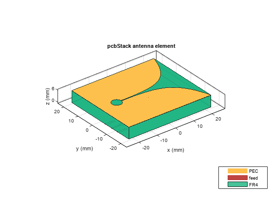
p.FeedLocations = [-0.0187 0 1 3];
figure;
show(p)
Multi-Layered dielectric pcbStack
There are two use cases for the PCBs with multiple dielectric layers; PCBs with dielectric layers present below the top metal layer or only above the top metal layer. Sections below describe how to define the BoardThickness for these two use cases.
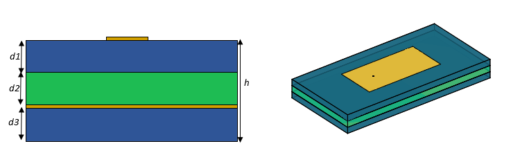
Dielectric layers present below the top metal layer
The BoardThickness of a PCB with multiple dielectric layers is the sum of thicknesses of all the dielectric layers present below the top metal layer. The dielectric layers above the top metal layer are considered as a coating and are not included in the board thickness calculations.
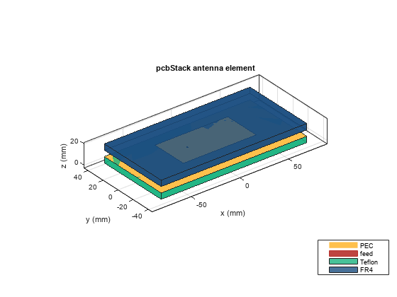
In the below use case, there are two dielectric layers between the top and bottom metal layers and one dielectric layer below the bottom metal layer as shown in the figure. The BoardThickness (h) for this PCB is the sum of the thicknesses (d1+d2+d3) of all the dielectric layers below the top metal layer.
p = pcbStack;
sub1 = dielectric('FR4');
sub2 = dielectric('Teflon');
TopMetal = p.Layers{1,1};
BtmMetal = p.Layers{1,2};

% Set the BoardThickness as sum of dielectric thickness below the top metal
% layer
h = 2*sub1.Thickness+sub2.Thickness;
p.BoardThickness = h;
p.Layers = {TopMetal,sub1,sub2,BtmMetal,sub1};
p.FeedLocations(1,3:4) = [1,4];
figure;
show(p)

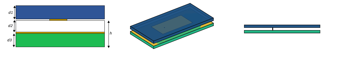
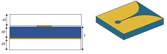
In the below use case, there is a dielectric layer present above the top metal layer and air dielectric separates the top and the bottom metal layers. There is another dielectric layer below the bottom metal layer. The dielectric layer which is present above the top metal layer is considered as coating and is not included in the BoardThickness calculation. The BoardThickness (h) is the sum of the thicknesses (d2+d3) of all the dielectric layers below the top metal layer.
p = pcbStack;
sub1 = dielectric('FR4');
sub2 = dielectric('Air');
sub3 = dielectric('Teflon');
TopMetal = p.Layers{1,1};
BtmMetal = p.Layers{1,2};

% Set the BoardThickness as sum of dielectric thickness below the top metal
% layer
h = sub2.Thickness+sub3.Thickness;
p.BoardThickness = h;
p.Layers = {sub1,TopMetal,sub2,BtmMetal,sub3};
p.FeedLocations(1,3:4) = [2,4];
figure;
show(p)
Dielectric layers present only above the top metal layer
In the below use case, the PCB has multiple dielectric layers only above the top metal layer. The BoardThickness (h) for this PCB is the sum of thicknesses (d1+d2) of all the dielectric layers. This is applicable only when there are no dielectric layers below the top metal layer.
p = pcbStack;
sub1 = dielectric('FR4');
sub2 = dielectric('Teflon');
TopMetal = p.Layers{1,1};

% Set the BoardThickness as sum of dielectric thickness below the top metal
% layer
h = sub1.Thickness+sub2.Thickness;
p.BoardThickness = h;
p.Layers = {sub1,sub2,TopMetal};
p.FeedLocations(1,3:4) = 3;
figure;
show(p)

Importing PCB design using pcbReader object
Import the top and bottom layers of the PCB from the Gerber file by setting .gtl and .gbl file to Layer2 and Layer4 in stackUp function. Pass the stackUp object to the PCBReader object.
S = stackUp;
S.Layer2 = 'UWBVivaldi.gtl';
S.Layer4 = 'UWBVivaldi.gbl';
p = PCBReader ('StackUp',S);
Create pcbStack of PCBReader object
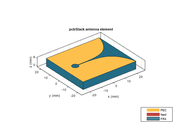
When the PCBReader object is converted into pcbStack, the pcbStack reads all the 5 layers of the stackUp object, where air dielectric is the default top and bottom layer. This is a multiple dielectric layers use case. Hence, the BoardThickness (h) is the sum of thicknesses (d2+d3) of the dielectric layers below the top metal layer.
pcb = pcbStack(p);
pcb.BoardThickness = pcb.Layers{3}.Thickness+pcb.Layers{5}.Thickness;
pcb.FeedLocations = [0,-5e-3,2]
pcb =
pcbStack with properties:
Name: 'UWBVivaldi'
Revision: 'v1.0'
BoardShape: [1×1 antenna.Rectangle]
BoardThickness: 0.0061
Layers: {[1×1 dielectric] [1×1 antenna.Polygon] [1×1 dielectric] [1×1 antenna.Polygon] [1×1 dielectric]}
FeedLocations: [0 -0.0050 2]
FeedDiameter: 0.0100
ViaLocations: []
ViaDiameter: []
FeedViaModel: 'square'
FeedVoltage: 1
FeedPhase: 0
Conductor: [1×1 metal]
Tilt: 0
TiltAxis: [1 0 0]
Load: [1×1 lumpedElement]
pcb.FeedDiameter = 0.1e-3;
show(pcb);
Modify the above use case by removing the top and bottom air dielectric layers as shown in figure below. This use case is now a single-layer dielectric pcbStack. Now you can change the dielectric Thickness (d) by changing the BoardThickess (h).
pcb = pcbStack(p);
d = pcb.Layers{3};
pcb.BoardThickness = d.Thickness;
L = {pcb.Layers{2},pcb.Layers{3},pcb.Layers{4}};
pcb.Layers = L;
pcb.FeedLocations = [0,-5e-3,1];
pcb.FeedDiameter = 0.1e-3;
show(pcb);