Transfer Nets in Serial Link Designer
Transfer nets are the primary net-class data structure in the Serial Link Designer app. They are common to both pre-layout and post-layout analysis. You can re-use the transfer nets in multiple ways from one phase of a project to another, or between projects.
In a serial link project, an interface contains a collection of signals such as clock, data, or strobes. These signals implement the physical layer protocol from the core one IC to the core of another IC. Each signal is called a transfer net. They consist of the drivers, receivers, electrical conductors and passive components involved in transmitting that signal type.
Edit Transfer Net Properties
To edit the transfer net properties, launch the Transfer Net Properties dialog box from Setup > TNet Properties.
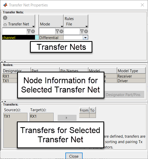
The dialog box contains:
list of all transfer nets in the current schematic set with their properties,
list of the model information for the selected transfer nets, and
transfers and transfer model overrides for selected transfer nets.
Transfer Nets
These are the basic properties for each transfer nets. They are listed in the Transfer Nets Properties dialog box.
| Column | Description |
|---|---|
| Transfer Net | The name of the transfer net. This is the same as the schematic sheet name in pre-layout. |
| Mode | The Mode is set to
|
| Rules File | Any rules files contained in the library. You can view the mask data for the selected rules file in the results table of the Signal Integrity Viewer app when viewing the analysis results. |
Nodes
Each node is listed as one row per designator.
| Column | Description |
|---|---|
| Designator | The name of the designator. |
| Part | The MathWorks Part name for the designator. |
| Pin Names | The names of the pins included in the designator. The pin names are from the IBIS component and IBIS file specified by the MathWorks Part. |
| Model | The default IBIS model for the designator. It is determined from the
precedence in the IBIS specification using the Pin entries and
Model Selector if present. |
| Model Type | The model type from the IBIS Model_Type parameter in the default IBIS model. |
You can edit the designator element properties or the designator parts, pins, or both.
Transfers
If a schematic sheet has multiple transmitters or receivers, transfers tell the Serial Link Designer app which transmitter (TX) goes to which receiver (RX). They are useful when the designator names are arbitrary. If the transmitters and receivers are numbered, the app automatically matches TX1 with RX1, TX2 with RX2, and so on.
To define a transfer, in the Transfer Net Properties dialog box, select a transmitter in the Source(s) parameter, select a receiver in the Target(s) parameter, and click the arrow button to create a new row.
Transfer Net in Pre-Layout Analysis
In pre-layout analysis, the Serial Link Designer app defines each transfer net on a separate schematic sheet and simulates in a separate simulation run. You can parameterize the circuit element values in a transfer net schematic. This allows you to evaluate many variations without changing the schematic. A transfer net schematic can also contain crosstalk interferers.
Transfer Net in Post-Layout Analysis
In post-layout analysis, each net on a PCB is called a CAD net. You can combine the CAD nets with drivers, receivers, packages, discrete components, and connector pins to form an extended net. An extended net contains designators, and reaches from one IC to another. Extended nets can also traverse multiple PCBs. You can identify individual extended nets and assign them to transfer nets for all major PCB flows.