STM32CubeMX Configuration for Voltage Mode Control
Click Launch in Configuration Parameters to open the selected STM32CubeMX project in STM32CubeMX tool.
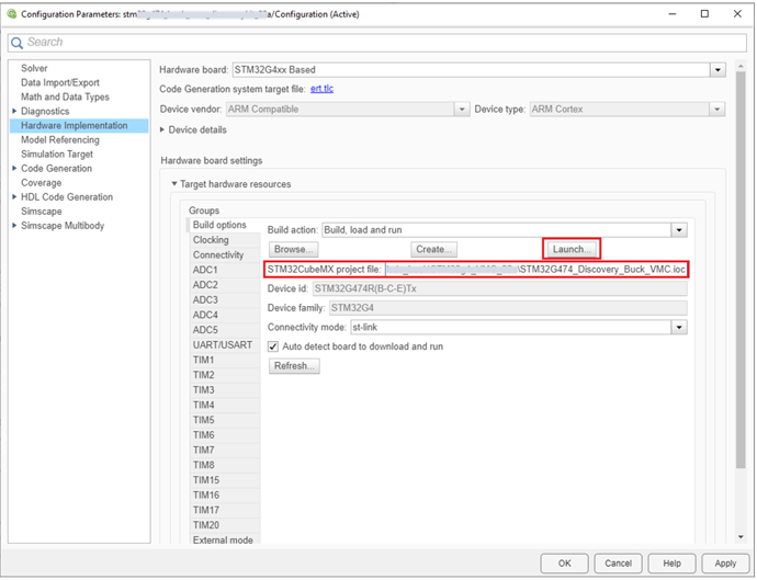
Open STM32CubeMX project and perform the following configurations.
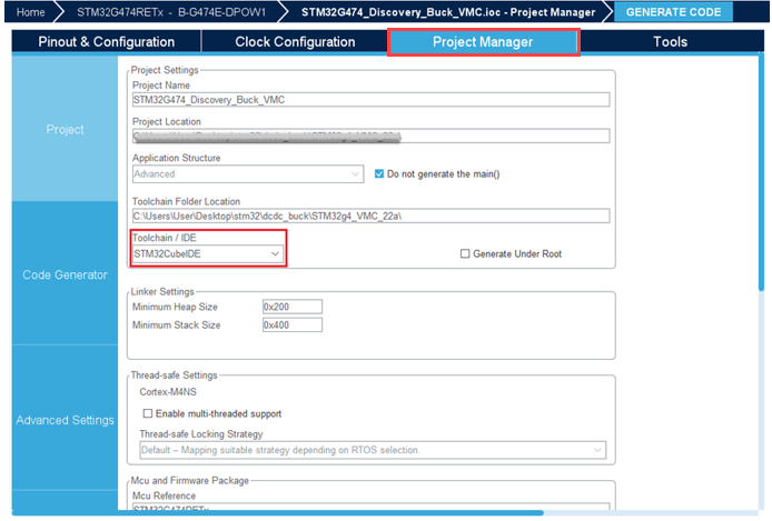
STM32CubeMX Project Manager Configuration
Select the preferred toolchain.
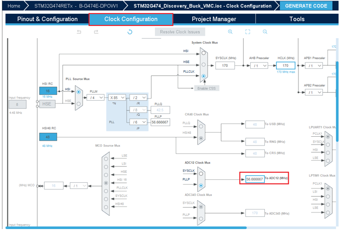
STM32CubeMX Clock Configuration
The ADC12 clock is set to
56.66MHz.HRTIM & USART3 clocks are set to
170MHz.
STM32CubeMX Pin Configuration
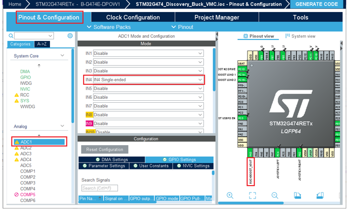
ADC Mode Settings
ADC Channel 4 (ADC_IN4) has the user label BUCKBOOST_VOUT and is
connected to PA3. This is the output voltage of the buck converter that is
regulated.
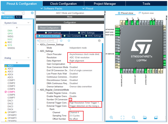
ADC Parameter Settings
Data Alignment is set to
Right
                alignment
. This stores the 12-bit result from the ADC in the 16-bit results register with the right alignment. That means the Lower12-bits (plus 1 sign bit) of the 16-bit register is used.Under the ADC_Regular_ConversionMode section, set the External Trigger Conversion Source to High-Resolution Trigger 1 event. Later set the External Trigger Conversion Edge to
Trigger detection on the rising edge.For the voltage mode buck converter, only one ADC conversion is required. This is the output voltage rail that is regulated. Therefore, the number of conversions is currently set to
1. The ADC conversion is configured by expanding the Rank subcategory.Set the Channel to
Channel 4.
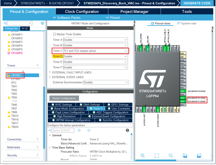
HRTIM Mode Settings
The High resolution timer module is configured to generate the PWM. The Buck power stage is driven by Timer C.
HRTIM Parameter Settings
Set the Period value to
27200with the resulting PWM period now calculated as200000Hz.Set Dead Time insertion to
Deadtime is inserted
                  between output 1 and output 2
. This enables the deadtime section which allows the outputs to be configured such that both high-side and low-side switches are never driven at the same time.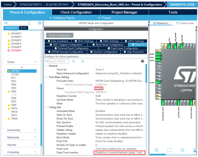
For Compare Unit 1 section change the configuration setting to
Enable. Enter a Compare Value of0. This is the initial value of the duty cycle fixed to0%.For Compare Unit 3 section change the configuration setting to
Enable. Enter a Compare Value of50. This is the event that is used to trigger the ADC sample. This can be moved to a clean point in the switching cycle, which means away from the turn-on or turn-off of the switch.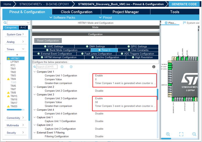
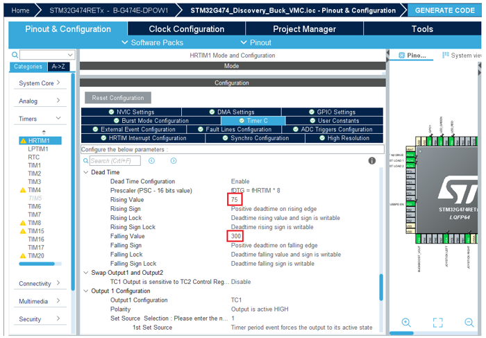
Set Rising Value to
75and Falling Value to300.The dead-time ticks fDTG are generated from fHRTIM and a prescaler:
fDTG = fHRTIM * 8, and
because fHRTIM = 170 MHz: fDTG = 170 MHz * 8 = 1360 MHz
therefore:
1 dead-time tick = 0.735 ns
Hence:
Rising value = 75 ticks = 55 ns Falling value = 300 ticks = 220 ns
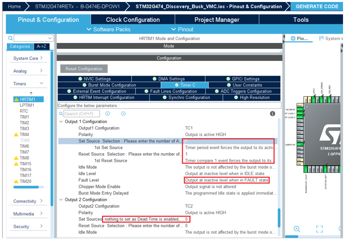
Under the Output 1 Configuration section, change the Set Source Selection number to
1. Change the 1st Set Source event toTimer period event forces the output to its active state.Change the Reset Source Selection number to
1. Change the 1st Reset Source event toTimer compare 1 event forces the output to its inactive state.Finally, set the Fault Level to
Output at the inactive level when in FAULT state.The Output 2 Configuration section is left unchanged as this output is driven by the dead-time.
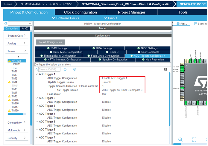
Enable the ADC Trigger 1 and set the Update Trigger Source to
Timer C, enter the number of Trigger Sources Selection to1. From the 1st Trigger Source drop-down, selectADC Trigger on Timer C compare 3.This is the event that triggers the ADC.
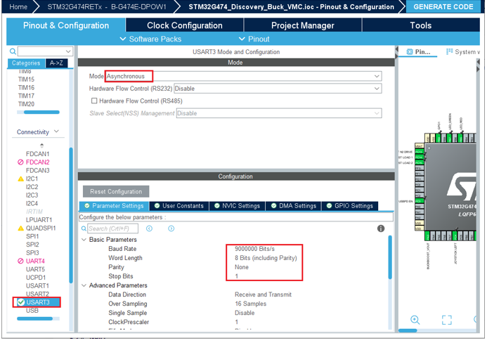
USART3 mode and configuration settings
Configure the USART3 for Host-Target communication.
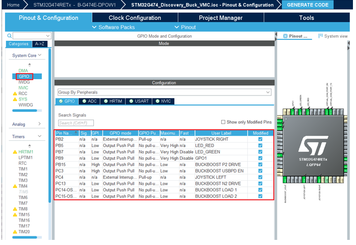
GPIO configuration settings
BUCKBOOST P2 DRIVE and BUCKBOOST N2 DRIVE are not used in the Buck-only configuration.
However, the BUCKBOOST P2 DRIVE must be High to support the Buck-only configuration.
BUCKBOOST USBPD EN would enable the input 5V to the power converter stage.
