Getting Started with STM32N6xx Based Microcontroller Series
R2026bThis example shows how to configure a Simulink® model for the STM32N6xx family of microcontrollers and deploy an application to the STMicroelectronics® NUCLEO-N657X0-Q board.
The STM32N6xx family is based on the ARM® Cortex®-M55 processor and includes the Neural-ART Accelerator™ for AI workloads. Unlike most STM32 devices, STM32N6xx microcontrollers do not contain internal flash memory. Instead, applications execute from internal SRAM (approximately, 4.2 MB). During deployment, the application is loaded into SRAM either by the ST-LINK® GDB server or through a First-Stage Boot Loader (FSBL) that copies the application from external XSPI flash memory.
In this example, you create and deploy a model that blinks the on-board green LED (LD1) on the NUCLEO-N657X0-Q board.
Choose an Execution Method
STM32N6xx devices support two execution methods. Select the method that best matches your development and deployment requirements.
Internal SRAM
Use the Internal SRAM execution method to deploy the application directly to internal SRAM. During deployment, the ST-LINK GDB server downloads the generated executable into SRAM and immediately starts execution.
This method is best suited for prototyping, testing, and rapid model iteration. Because SRAM is volatile, the application is removed when power is disconnected. When using this execution method, configure all peripherals in the FSBL runtime context in STM32CubeMX.
Load and Run (LRUN) from External Memory
Use the Load and Run (LRUN) execution method when the application must persist across power cycles. In this mode, the application is stored in external XSPI flash memory and copied to internal SRAM during boot.
The FSBL performs the boot-time initialization and loads the application into SRAM before execution begins. Configure model-level peripherals in the Application runtime context and configure the boot path components, such as XSPIM, XSPI, and EXTMEM_MANAGER, in the FSBL runtime context.
Prerequisites
If you are new to Simulink, we recommend completing the Simulink Onramp interactive tutorial to get started.
Watch this STM32CubeMX GPIO configuration video for an introduction to STM32CubeMX.
Both the workflows in this example use STM32CubeMX to configure board peripherals and generate initialization code for the STM32N6xx device. You can either create a new STM32CubeMX project or use an existing project file (.ioc). Simulink allows you to open and modify the STM32CubeMX project directly from the model configuration settings. For more information, see STM32CubeMX overview.
Required Hardware
To run this example, you need the following hardware:
USB Type‑C cable
NUCLEO‑N657X0‑Q board
GPIO Assignments
The example uses the following pins:
PC13 - GPIO Input (User Button B1) - Enable an internal pull‑down resistor because the user button is active‑high on this board
PG0 - GPIO Output (Green LED, LD1)
PE5 / PE6 - USART1 TX / RX (ST‑LINK Virtual COM Port, used for External Mode)
Run Hardware Board Setup
Run the following command in the MATLAB Command Window to launch the Hardware Setup wizard. Follow the guided steps to register the STMicroelectronics software tools needed for code generation and deployment.
stm32setup
Select STM32N6xx Based MCUs to add support for the STM32N6xx MCU family.
Workflow 1: Deploy to Internal SRAM
Use this workflow to build and execute the application directly from internal SRAM. In this workflow, you use the preconfigured project file stm32n6_gettingstarted_sram.ioc and then complete the remaining hardware and model configuration steps.
Run this command to open the model:
open_system("stm32n6_gettingstarted.slx")Configure the Simulink Model
1. Open Configuration Parameters by pressing Ctrl+E.
2. Navigate to Hardware Implementation > Hardware board, and select STM32N6xx Based.
3. Under Build options tab, select the provided STM32CubeMX project:stm32n6_gettingstarted_sram.ioc
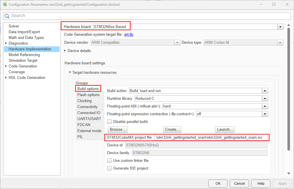
4. Under Flash options, set Execution method to Internal SRAM.
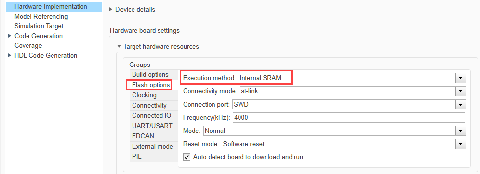
With this setting, when you build and deploy the model, Simulink downloads the executable directly into SRAM and starts execution without programming external flash memory.
Configure the STM32CubeMX Project
Launch STM32CubeMX from Simulink and configure the required peripherals.
Configure GPIO Pins
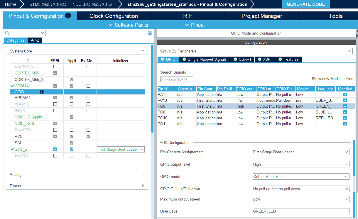
Configure the following pins in the FSBL runtime context.
Pin | Mode | Label |
PG0 | GPIO_Output | GREEN_LED |
PC13 | GPIO_Input | USER_SWITCH |
For PG0, configure:
Pin Context Assignment: FSBL
GPIO Output Level: Low
GPIO Mode: Output Push Pull
Pull-up/Pull-down: No pull-up and no pull-down
Output Speed: Low
For PC13, configure:
Pin Context Assignment: FSBL
GPIO Mode: Input
Pull-up/Pull-down: Pull-down
User Label: USER_SWITCH
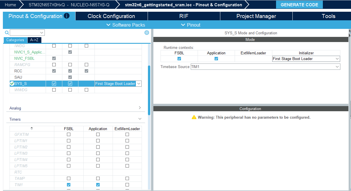
Configure the System Time Base
Open System Core > SYS_S.
Enable FSBL as the runtime context.
Set Timebase Source to TIM1.
Configure External Mode Communication
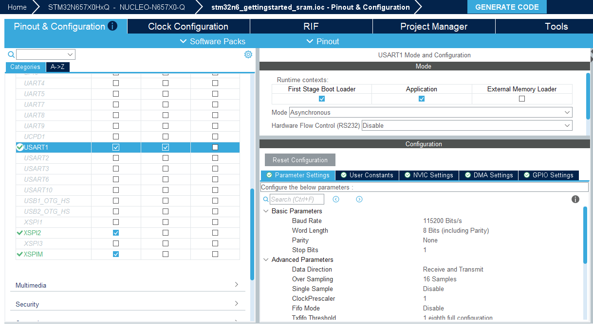
External Mode (used by Simulink to monitor signals and tune parameters at run time) needs a USART connected to a DMA channel. On the NUCLEO‑N657X0‑Q the on‑board ST‑LINK Virtual COM Port is wired to USART1 (PE5 = TX, PE6 = RX).
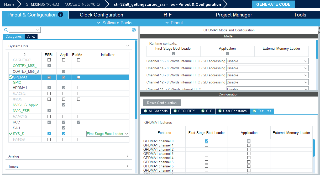
Configure USART1 and GPDMA1 for External Mode communication.
For Connectivity > USART1:
Mode: Asynchronous
Runtime Context: FSBL
Use the default 115200 8N1 settings (External Mode re-configures the baud rate at run time).
For System Core > GPDMA1:
Enable Channel 0
Assign the channel to USART1 TX
Use secure and privileged attributes
Verify Resource Isolation Framework Settings
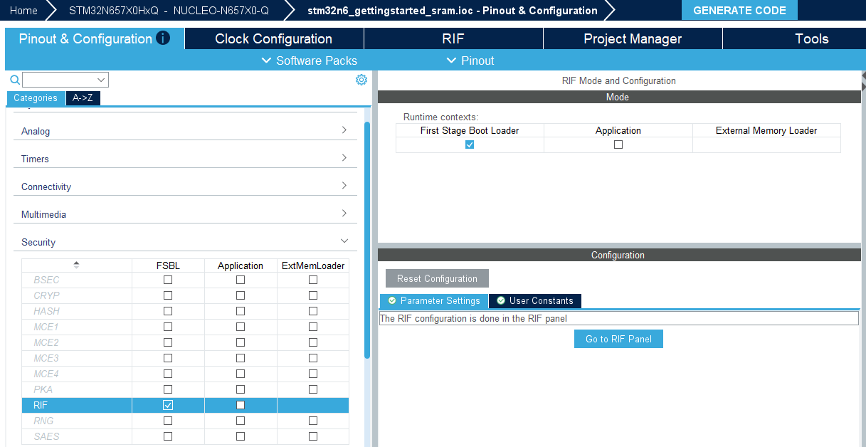
The STM32N6xx family uses the Resource Isolation Framework (RIF) to manage access to peripherals and GPIO pins across runtime and security contexts. The RIF defines which context can access each hardware resource.
Because this workflow executes entirely in the FSBL runtime context, STM32CubeMX automatically assigns the required RIF permissions when you configure peripheral and pin ownership. Therefore, you typically do not need to modify the default RIF settings.
Open Pinout & Configuration > Security > RIF and verify that the the First Stage Boot Loader context is selected. All peripherals used in this example, such as GPIO, USART1, GPDMA1, and TIM1, appears under the FSBL column.
Configure Project Settings
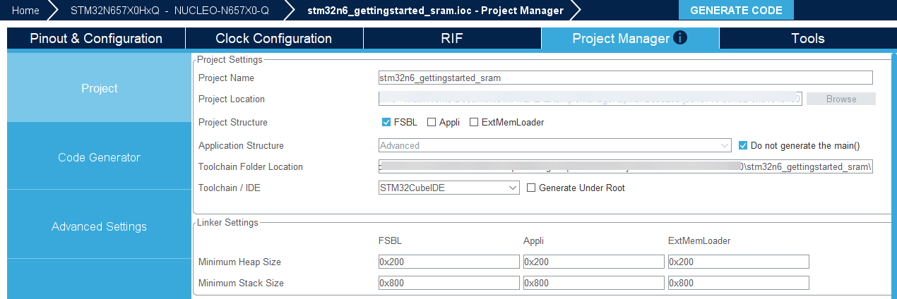
In Project Manager, configure:
Project Name: stm32n6_gettingstarted_sram
Project Structure: Select only FSBL
Application Structure: Select Do not generate the main()
Toolchain: STM32CubeIDE
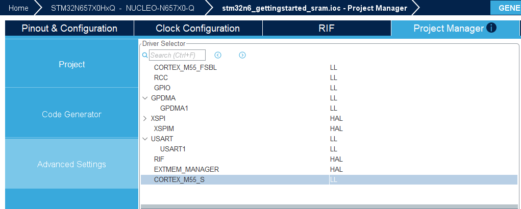
In Project Manager > Advanced Settings > Driver Selector, configure the following drivers to use the LL layer:
CORTEX_M55
RCC
GPIO
USART
GPDMA
Build and Deploy the LED Blink Application
Open the Simulink model:
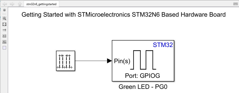
open_system("stm32n6_gettingstarted.slx");The model uses a Digital Port Write block to control the GPIO pin connected to the green LED on the NUCLEO-N657X0-Q board.
Configure the Digital Port Write Block
Configure the desired GPIO pin using these block parameters:
Port name: GPIOG
Pin number: 0
Select Access port pins as array
Build and Deploy
Press CTRL+B or click the Build, Deploy & Start button on the Hardware tab to generate code and deploy to the board.
Observe the green LED blinking on the NUCLEO‑N657X0‑Q board.
To view build diagnostics and generated code, see the Diagnostic Viewer.
Workflow 2: Deploy by Using Load and Run (LRUN)
Use the Load and Run (LRUN) execution method when you want the application to persist across power cycles.
Unlike most STM32 microcontrollers, the STM32N6xx family does not include internal flash memory. Instead, user applications are stored in external flash memory and executed from internal SRAM. During startup, the boot process copies the application from external flash into SRAM before execution begins.
In LRUN mode, the boot ROM first loads a First-Stage Boot Loader (FSBL) from external flash into SRAM. The FSBL then initializes the system, loads the application into SRAM, and starts execution.
The LRUN startup sequence consists of the following stages:
On reset, the boot ROM reads the BOOT0 and BOOT1 pin states to determine the boot source.
The boot ROM copies the FSBL image from external XSPI flash memory into an internal SRAM download buffer and transfers control to the FSBL.
The FSBL initializes system clocks, configures the XSPIM routing and XSPI peripheral, and starts the External Memory Manager middleware.
The External Memory Manager copies the application image from external flash to the configured SRAM destination address.
The FSBL transfers control to the application entry point, and the Simulink-generated code begins execution from SRAM.
XSPI and External Flash Memory
The STM32N6xx family accesses external flash memory through the XSPI (eXtensible SPI) peripheral.
XSPI supports multiple memory interfaces, including:
Quad SPI (4 data lines)
Octo SPI (8 data lines)
Hexadeca SPI (16 data lines)
XSPI can communicate with NOR flash devices from manufacturers such as Macronix, Micron, and AP Memory.
The STM32N6xx family provides three XSPI instances: XSPI1, XSPI2, and XSPI3. An XSPIM (XSPI Manager) routing multiplexer maps these XSPI instances to the available physical ports.
LRUN in STM32CubeMX Project Structure
An LRUN project in STM32CubeMX contains two runtime contexts that work together during boot and execution.
FSBL Context - The First-Stage Boot Loader (FSBL) runs first after the boot ROM loads it into SRAM. The FSBL initializes the system, configures the external memory interface, and launches the application through the External Memory Manager middleware. Configure the following components in the FSBL context: XSPIM, XSPI, EXTMEM_MANAGER.
Application Context - The Application project contains the user application stored in external flash memory. During startup, the FSBL copies the application into SRAM and transfers control to it. Configure model-level peripherals, such as GPIO and USART, in the Application context.
External Memory Manager
The External Memory Manager middleware provides a common interface for accessing external memory devices and includes boot services for loading and starting the application. An external loader (.stldr) is a device-specific programming utility that STM32CubeProgrammer loads into SRAM during flashing operations. The loader contains the information required to erase, program, and verify a specific flash memory device.
For the NUCLEO-N657X0-Q board, STMicroelectronics provides a preconfigured external loader file named MX25UM51245G_STM32N6570-NUCLEO.stldr. This loader supports the on-board Macronix MX25UM51245GXDI00 OctoSPI flash device and is installed with STM32CubeProgrammer in <STM32CubeProgrammer install path>\bin\ExternalLoader\.
The loader name typically indicates the flash device it supports. If your custom hardware uses a different flash memory device, select a compatible loader or provide a custom .stldr file. In Simulink, use the Custom loader option in the Flash options settings to specify your own loader.
Configure the Simulink Model for LRUN
Run this command to open the multi-rate Simulink model:
open_system("stm32n6_gettingstarted_multirate.slx")In this workflow, you use the preconfigured project file stm32n6_gettingstarted_lrun.ioc and then complete the remaining hardware and model configuration steps.
1. Open Configuration Parameters by pressing Ctrl+E.
2. Navigate to Hardware Implementation > Hardware board, and select STM32N6xx Based.
3. Under Build options tab, select the provided STM32CubeMX project:stm32n6_gettingstarted_lrun.ioc
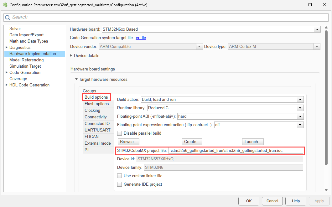
4. Under Flash options, set Execution method to Load and Run (LRUN) from external memory.
5. For the NUCLEO-N657X0-Q board, select the external loader: MX25UM51245G_STM32N6570-NUCLEO.stldr.
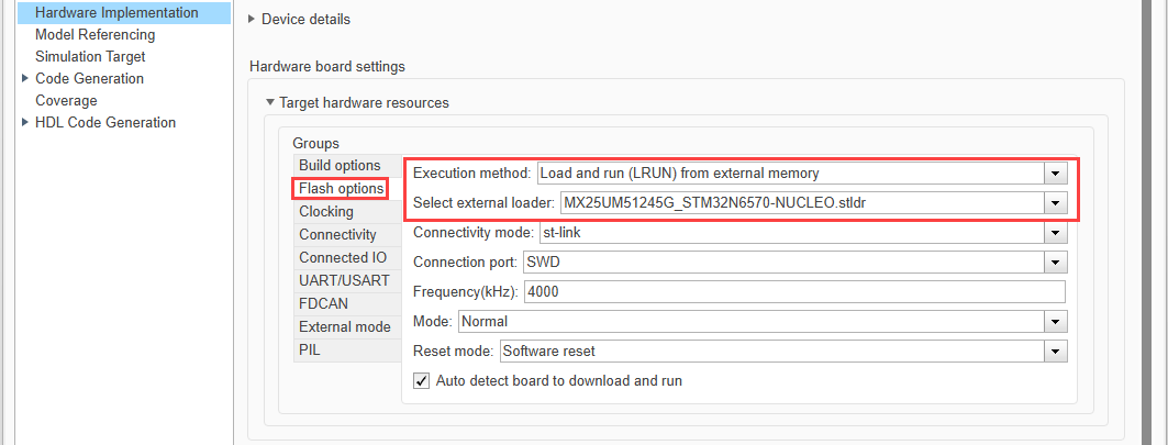
Note: STM32CubeProgrammer includes external loaders for many ST evaluation boards and supported flash memory devices, which you can select directly from the loader list. For custom boards, ensure that the selected .stldr file supports the external flash memory device installed on the board. If your flash device is not supported by the loaders included with STM32CubeProgrammer, create or obtain a compatible .stldr file and specify it using the Custom loader option in the Flash options settings.

Configure the STM32CubeMX Project
Launch STM32CubeMX from Simulink and configure the required peripherals.
The LRUN workflow requires configuration of the external memory interface in the FSBL context and the application peripherals in the Application context.
You must configure peripherals in the following order:
XSPIM → XSPI2 → EXTMEM_MANAGER
XSPI2 depends on XSPIM routing, and EXTMEM_MANAGER depends on XSPI2. Configuring these components out of sequence can result in missing configuration options or incorrect default settings.
Configure XSPIM
The XSPI Manager (XSPIM) determines which XSPI instance connects to which physical port.
Open Pinout & Configuration > Connectivity > XSPIM, and configure:
Runtime Context: FSBL
Mode: Direct
Direct mode maps XSPI1 to Port 1, and XSPI2 to Port 2.
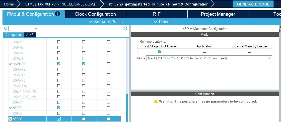
For the NUCLEO-N657X0-Q board, this configuration is required because the MX25UM51245GXDI00 flash memory is connected to Port 2 pins (PN0-PN12).
For custom hardware, determine the correct XSPIM routing by examining the schematic and identifying which physical port is connected to the flash memory device.
Configure XSPI2
Open Pinout & Configuration > Connectivity > XSPI2, and configure:
Runtime Context: FSBL
Mode: Octo SPI
Chip Select Override: NCS1 - Port2
Memory Type: Macronix
Memory Size: 1 Gbits
Chip Select High Time Cycle: 1
Delay Hold Quarter Cycle: Enable
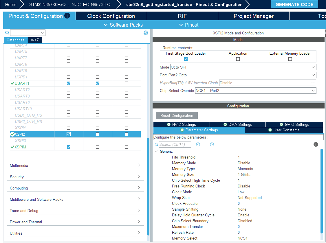
STM32CubeMX automatically assigns the required GPIO pins. For the NUCLEO-N657X0-Q board, verify that PN0-PN12 are assigned to the XSPI interface and match the board schematic.
Configure SYS_S and the Time Base
Both the FSBL and the Application require a HAL time base.
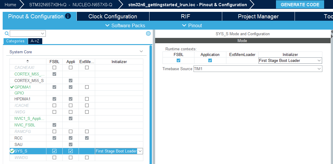
Open Pinout & Configuration > System Core > SYS_S, and configure the following:
Enable both FSBL and Application runtime contexts.
Set Initializer to First Stage Boot Loader.
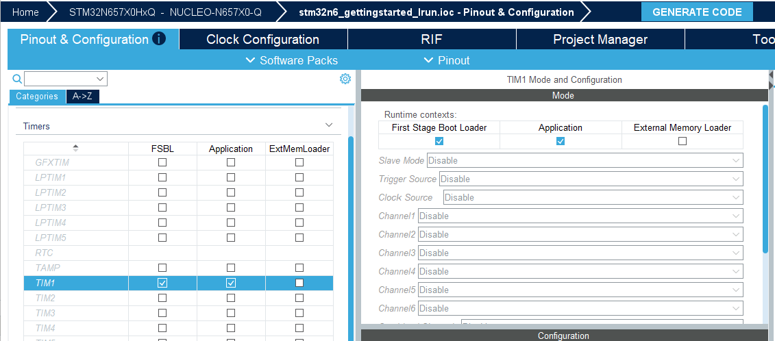
Set Timebase Source to a hardware timer such as TIM1. Do not use SysTick as the HAL time base because SysTick is reserved for the RTOS scheduler.
In the Timers section, verify that the selected timer is enabled in both the FSBL and Application columns.
Configure the External Memory Manager
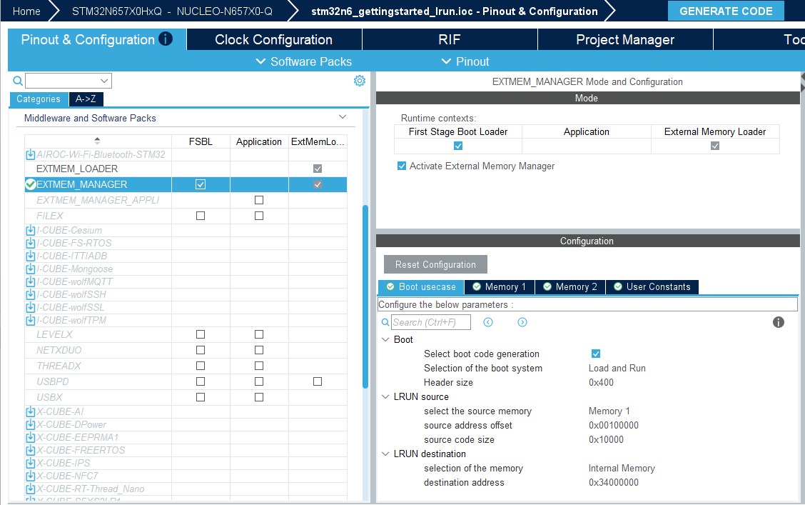
Open Pinout & Configuration > Middleware and Software Packs > EXTMEM_MANAGER.
Enable the boot configuration by performing these steps:
Select Activate External Memory Manager.
Select Select boot code generation.
Set Selection of boot system to Load and Run.
Configure LRUN Parameters for EXTMEM_MANAGER
Configure:
Source Memory: Memory 1
Source Address Offset: 0x00100000
Source Code Size: 0x10000
Destination Memory: Internal Memory
Destination Address: 0x34000000
The application image is programmed at address 0x70100000, which corresponds to the XSPI2 base address plus the 1 MB offset (XSPI2 base 0x70000000 + offset 0x00100000). Using a different offset causes the boot code to load the application from the wrong flash location.
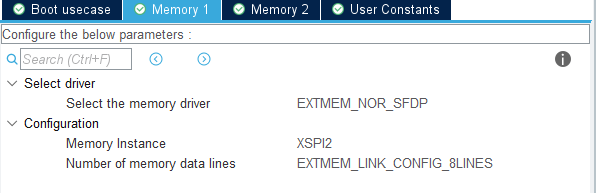
In the Memory 1 tab, configure:
Driver: EXTMEM_NOR_SFDP. This driver uses the JEDEC SFDP standard to auto‑detect flash characteristics at runtime, and works with most modern NOR flash ICs. For custom boards, if your flash does not support SFDP, select the manufacturer‑specific driver instead (for example, EXTMEM_NOR_MACRONIX)
Memory Instance: XSPI2. On the NUCLEO‑N657X0‑Q, the flash is on the XSPI2 power domain (VDD_OCTO2_M on schematic MB1940). This must match the XSPI peripheral. For custom boards, select the XSPI instance matching your schematic (check the VDD_OCTOx_M power rail supplying your flash).
Number of Memory Data Lines: EXTMEM_LINK_CONFIG_8LINES. On the NUCLEO‑N657X0‑Q, the MX25UM51245G is an Octo‑SPI flash with 8 data lines (IO0–IO7 routed on schematic). For custom boards, check your flash datasheet for the supported interface width, and verify how many lines are physically routed on your PCB, and select the corresponding option (4LINES or 8LINES).
Hardware References
While configuring XSPI and EXTMEM_MANAGER for a custom board, refer to the following documents to determine the correct settings:
Board User Manual (UM3417 for NUCLEO‑N657X0‑Q) — Section 7.10 identifies the flash memory specifications (size, voltage, frequency, interface type) and confirms the XSPI connection.
Board Schematic (MB1940 for NUCLEO‑N657X0‑Q) — The "OctoSPI Flash" sheet shows the flash IC part number, XSPI power domain (VDD_OCTO2_M → XSPI2), pin routing (PN0–PN12), and chip‑select connections.
Flash IC Datasheet (MX25UM51245G for NUCLEO‑N657X0‑Q) — Provides the memory type (Macronix), capacity (512 Mbit), interface width (Octo SPI, 8 lines), voltage (1.8 V), maximum frequency (200 MHz), and timing parameters (tSHSL for Chip Select High Time).
STM32N6 Reference Manual (RM0486) — Memory map section provides XSPI base addresses: XSPI1=0x90000000, XSPI2=0x70000000, XSPI3=0x80000000.
Configure Project Settings
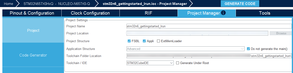
In Project Manager, configure:
Project Name:
stm32n6_gettingstarted_lrunProject Structure: FSBL and Appli
Application Structure: Select Do not generate the main()
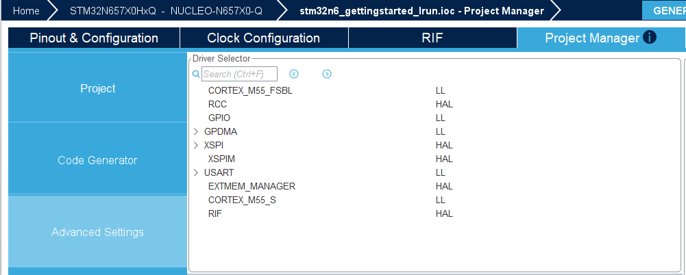
In Project Manager > Advanced Settings > Driver Selector, configure the following drivers to use the LL layer:
CORTEX_M55
RCC
GPDMA
GPIO
USART
Configure the following drivers to use the HAL layer:
XSPI
XSPIM
EXTMEM_MANAGER
RIF
Configure Application Peripherals
Because the application executes in the Application context, configure user peripherals (GPIO, GPDMA1, and USART1) in that context.
Additionally, configure PC13 as GPIO Input with Pull-down, and PG0 as GPIO Output.
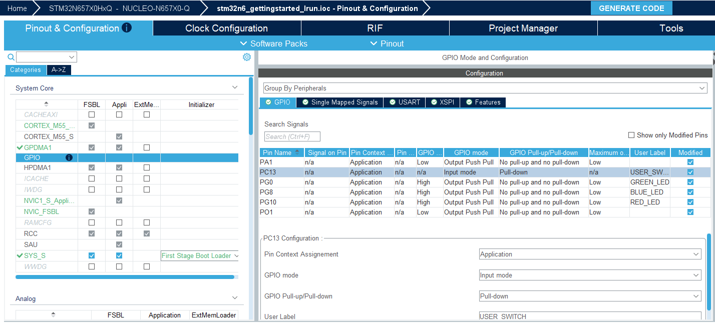
STM32CubeMX automatically updates the RIF configuration when ownership changes so that the Application context can access these resources.
Build and Deploy the Multi-rate LED Blink Application
Open the Simulink model:
open_system("stm32n6_gettingstarted_multirate.slx");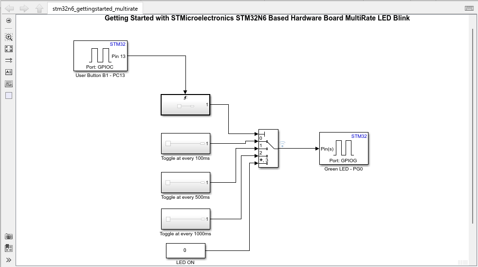
Configure the Blocks
Configure the Digital Port Read and Digital Port Write blocks in the model for the desired GPIO pins.
Digital Port Read (User Button): Port GPIOC, Pin 13
Digital Port Write (Green LED): Port GPIOG, Pin 0
The model reads the user button, and each button press advances the green LED between blink rates (100 ms, 500 ms, 1000 ms).
Build and Deploy
Press CTRL+B or click the Build, Deploy & Start button on the Hardware tab to generate code and deploy to the board.
Simulink builds two binaries — the FSBL image and the Application image — and launches the STM32 Deployer Screen window to program them into external XSPI flash. Follow the instructions in this three‑step wizard.
The STM32N6xx boot ROM uses the BOOT0 and BOOT1 pins to determine how to start the device.
DEV Boot Mode is used while programming the device. STM32CubeProgrammer loads the external loader and programs the FSBL and Application images into external flash.
Flash Boot Mode is used during normal execution. The boot ROM loads the FSBL from external flash, and the FSBL loads the Application into SRAM.
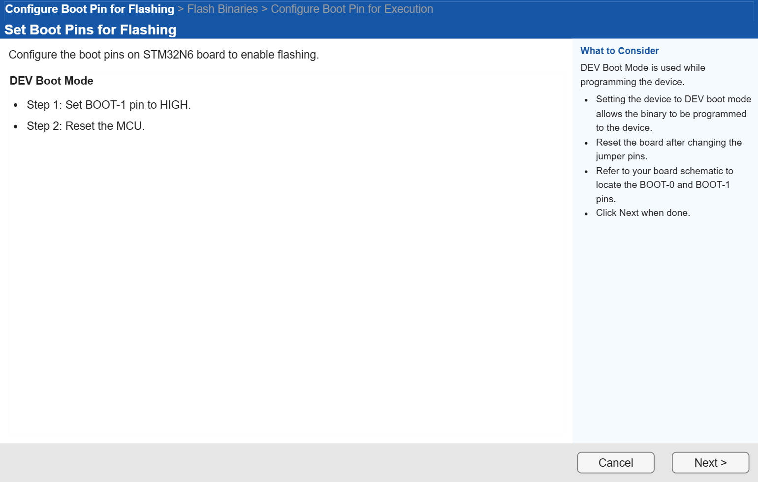
Set Boot Pins for Flashing
To enter DEV Boot Mode:
Set BOOT1 to HIGH.
Reset the MCU.
Click Next.
Flash Binary to Device
In this window, click Flash Binaries.
The deployer programs both the FSBL and Application images into external flash memory. A green check mark indicates successful programming.
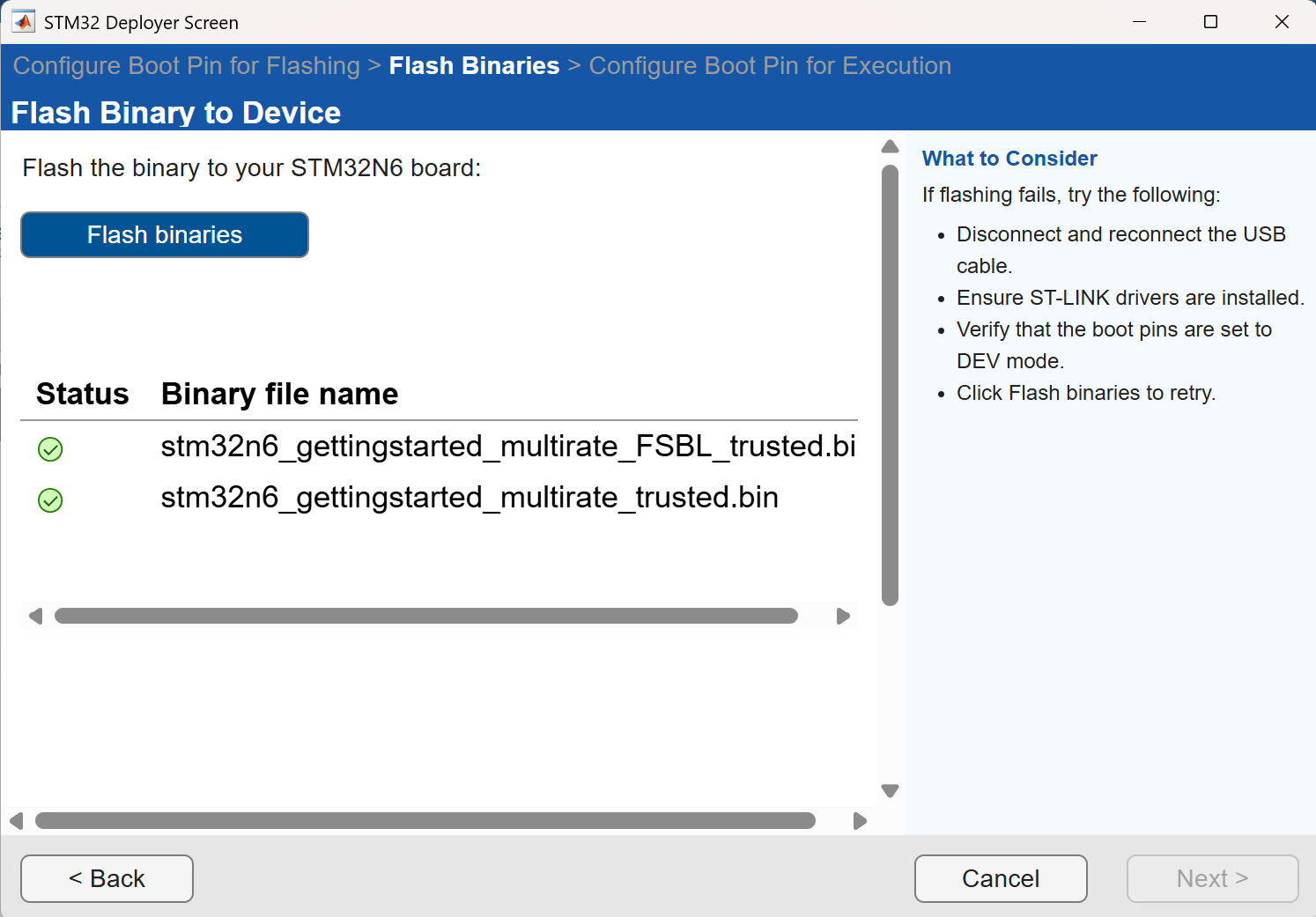
If programming fails:
Reconnect the USB cable.
Verify that the ST-LINK drivers are installed.
Confirm that the board is in DEV Boot Mode.
Retry the flashing operation.
When programming completes, click Next.
Configure Boot Pins for Execution
To enter Flash Boot Mode:
Set BOOT0 to LOW.
Set BOOT1 to LOW.
Reset the MCU.
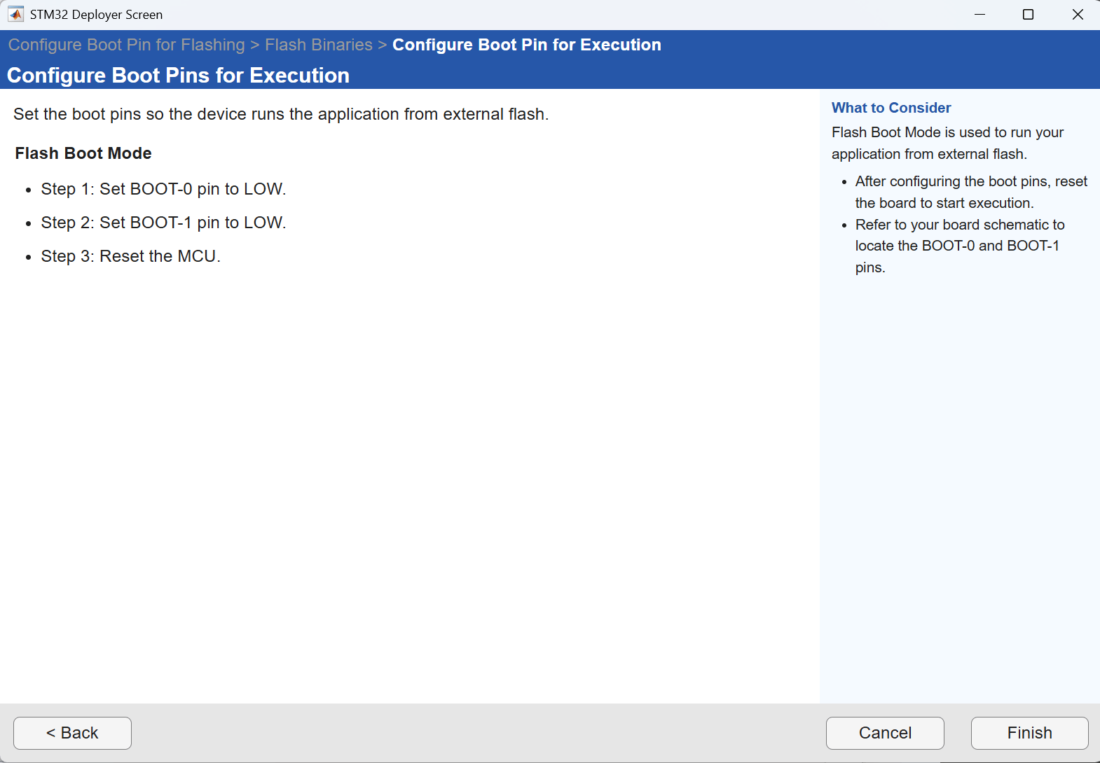
After reset, the boot ROM loads the FSBL from external flash, the FSBL loads the Application into SRAM, and the application begins running. Press the B1 user button to cycle the green LED through the configured blink rates.
Review Block Library for STM32N6xx Series
You can explore all the blocks available for the STM32N6xx series by opening the corresponding Simulink Library Browser:
open_system('stm32n6xxblockslib');Other Things to Try
Configure a Hardware Interrupt block to generate an ISR that runs in response to the user button (EXTI13) instead of polling PC13.
Use the Digital Port Read block to read the user button (PC13) and control LED behavior based on button press.

