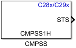
C28x/C29x CMPSS
Compare two input voltages on comparator pins
Libraries:
C2000 Microcontroller Blockset /
F280013x
C2000 Microcontroller Blockset /
F280015x
C2000 Microcontroller Blockset /
F28002x
C2000 Microcontroller Blockset /
F28003x
C2000 Microcontroller Blockset /
F28004x
C2000 Microcontroller Blockset /
F2807x
C2000 Microcontroller Blockset /
F2837xD
C2000 Microcontroller Blockset /
F2837xS
C2000 Microcontroller Blockset /
F2838x /
C28x
C2000 Microcontroller Blockset /
F28p65x
C2000 Microcontroller Blockset /
F28p55x
C2000 Microcontroller Blockset /
F29H85x
Description
The Comparator Subsystem consists of two modules, Comparator High (COMPH) and Comparator Low (COMPH). Each module generates a high digital output when the voltage on the first input pin (positive input) is greater than the voltage on the second input pin (negative input). And each module generates a low digital output when the voltage on the first input pin (positive input) is less than the voltage on the second input pin (negative input).
The second input pin can either be the external pin or the DAC module.
Ports
Input
Output
Parameters
Configuration of GPIO as Analog Pins
For TI F280013x and TI F280015x processors the following tables provides the mapping of GPIO pins which can be used as the analog pins for ADC and CMPSS blocks.
| GPIO | ADC | CMPSS | ||
| Module | Channel | Module | Input | |
| GPIO12 | A | 20 | ||
| C | 20 | |||
| GPIO13 | A | 19 | ||
| C | 19 | |||
| GPIO20 | A | 17 | ||
| C | 17 | |||
| GPIO21 | A | 18 | ||
| C | 18 | |||
| GPIO28 | A | 16 | ||
| C | 16 | |||
| GPIO224 | A | 2 | 1 | Positive |
| C | 9 | |||
| GPIO226 | C | 6 | 3 | Positive |
| GPIO227 | A | 9 | 2 | Positive |
| C | 8 | 4 | Positive | |
| GPIO228 | A | 6 | 1 | Positive |
| GPIO230 | A | 10 | 2 | Negative |
| C | 10 | |||
| GPIO242 | A | 3 | 3 | Negative |
| C | 5 | |||
For TI F28P65x processors the following tables provides the mapping of GPIO pins which can be used as the analog pins for ADC and CMPSS blocks.
| GPIO | ADC | CMPSS | |||
| Module | Channel | Module | Input | ||
| GPIO198 | B | 31 | 11 | Positive | |
| C | 7 | ||||
| GPIO199 | B | 24 | 6 | Positive | |
| C | 0 | 6 | Negative | ||
| GPIO200 | B | 25 | 6 | Positive | |
| C | 1 | ||||
| GPIO201 | C | 9 | 11 | Positive | |
| GPIO202 | C | 8 | 10 | Positive | |
| GPIO203 | B | 30 | 10 | Positive | |
| C | 6 | ||||
| GPIO204 | B | 25 | 2 | Positive | |
| C | 9 | 5 | Negative | ||
| GPIO205 | B | 28 | 5 | Positive | |
| C | 4 | 10 | Negative | ||
| GPIO206 | B | 27 | 3 | Positive | |
| C | 3 | 6 | Negative | ||
| GPIO207 | A | 30 | 7 | Positive | |
| B | 6 | 7 | Negative | ||
| GPIO208 | A | 31 | 3 | Negative | |
| B | 7 | 7 | Positive | ||
| GPIO209 | A | 6 | 7 | Positive | |
| GPIO210 | 4 and 9 | Positive | |||
| A | 7 | 7 | Negative | ||
| GPIO211 | A | 8 | 8 | Positive | |
| C | 24 | ||||
| GPIO212 | A | 9 | 5 | Positive | |
| C | 25 | 8 | Negative | ||
| GPIO213 | A | 10 | 8 | Positive | |
| C | 26 | 8 | Negative | ||
| GPIO214 | A | 11 | 8 | Positive | |
| C | 27 | ||||
| GPIO215 | A | 28 | 5 | Positive | |
| B | 4 | 5 | Negative | ||
| GPIO216 | A | 25 | 5 | Positive | |
| B | 5 | ||||
| GPIO217 | B | 8 | 2 | Positive | |
| C | 28 | 10 | Negative | ||
| GPIO218 | B | 9 | 2 | Positive | |
| C | 29 | 9 | Negative | ||
| GPIO219 | B | 10 | 4 | Positive | |
| C | 30 | 4 | Negative | ||
These pins are configured as analog pins if ADC or CMPSS blocks utilize them. Ensure that a GPIO pin is not used as both digital and analog pin. For example, if GPIO12 cannot be used in digital input or digital output block and as ADCA input channel 20.
Note
In some C28x processors, the GPIO pin selection for CMPSS blocks is done by
configuring CMPHPMXSEL, CMPLPMXSEL,
CMPHNMXSEL, and CMPLNMXSEL registers. Use the
Register Read/Write block in Initialize function
subsystem to write to these registers. For example, to use AIO233 as CMPSS1
Positive input for COMPH and COMPL, use Register Read/Write block in Initialize function
subsystem to write to 3 to
AnalogSubsysRegs.CMPHPMXSEL.bit.CMP1HPMXSEL and
AnalogSubsysRegs.CMPLPMXSEL.bit.CMP1LPMXSEL bits.
Version History
Introduced in R2020a
