stackUp
R2026bCreate PCB stackup definition
Description
Use the stackUp object to create a printed circuit board
(PCB) stackup definition to import Gerber files. A Gerber file is a set of manufacturing files
used to describe a PCB antenna. A Gerber file uses an ASCII vector format for 2-D binary
images.
Creation
Description
s = stackUp creates a PCB stackUp object with
a default of 2 metal layers and at least 5 total layers arranged as
dielectric–metal–dielectric–metal–dielectric. Metal layers (layers 2 and 4) accept
Gerber files, while dielectric layers (layers 1, 3, and 5) accept
dielectric objects.
s = stackUp( creates
a PCB NumMetalLayers=Value)stackUp object with the number of metal layers specified by
Value. The stackUp object arranges layers in an
alternating dielectric–metal pattern, starting and ending with dielectric layers.
Odd-indexed layers are dielectric, and even-indexed layers are metal. The total number
of layers is computed as 2 × NumMetalLayers + 1, with a minimum of
five layers. Unused metal layers remain empty.
Properties
Examples
Create a default PCB stackup definition object.
s = stackUp;
Create a dielectric object with Air as the dielectric material and with a thickness of 0.1 mm.
d1 = dielectric("Air");
d1.Thickness = 0.1e-3;
Create another dielectric object with RO4725JXR as the dielectric material.
d3 = dielectric("RO4725JXR");Assign the dielectrics to the first and third layers.
s.Layer1 = d1;
s.Layer3 = d3;
Input Gerber files to the second and fourth layers.
s.Layer2 = "antenna_design_file.gtl";
s.Layer4 = "antenna_design_file.gbl";
Display the stackup definition object.
s
s =
  stackUp with properties:

    NumMetalLayers: 2
         NumLayers: 5
            Layer1: [1×1 dielectric]
            Layer2: "antenna_design_file.gtl"
            Layer3: [1×1 dielectric]
            Layer4: "antenna_design_file.gbl"
            Layer5: [1×1 dielectric]
Create a stackUp object with three metal layers. Assign Gerber files to the metal layers.
s = stackUp(NumMetalLayers=3);
s.Layer2='TopLayer.gtl';
s.Layer4='InnerCopperLayer.g2l';
s.Layer6='BottomLayer.gbl'
s =
  stackUp with properties:

    NumMetalLayers: 3
         NumLayers: 7
            Layer1: [1×1 dielectric]
            Layer2: 'TopLayer.gtl'
            Layer3: [1×1 dielectric]
            Layer4: 'InnerCopperLayer.g2l'
            Layer5: [1×1 dielectric]
            Layer6: 'BottomLayer.gbl'
            Layer7: [1×1 dielectric]
Use the PCBReader object to import the PCB layout defined in the stackUp object. Specify the drill file and layer connectivity.
p = PCBReader(StackUp=s);
p.DrillLayerPairs = [1,3];
p.DrillFile = {'drillFile.txt'};
Convert the design into a PCB antenna using the pcbStack object. Define the feed properties.
pcbAnt = pcbStack(p);
pcbAnt.FeedDiameter = 0.5e-3;
pcbAnt.FeedLocations = [-5e-3 5e-3 2]
pcbAnt =
  pcbStack with properties:

              Name: 'TopLayer'
          Revision: 'v1.0'
        BoardShape: [1×1 antenna.Rectangle]
    BoardThickness: 0.0121
            Layers: {[1×1 dielectric]  [1×1 antenna.Polygon]  [1×1 dielectric]  [1×1 antenna.Polygon]  [1×1 dielectric]  [1×1 antenna.Polygon]  [1×1 dielectric]}
        FeedFormat: 'FeedLocations'
     FeedLocations: [-0.0050 0.0050 2]
      FeedDiameter: 5.0000e-04
      ViaLocations: [-0.0060 0.0071 2 6]
       ViaDiameter: 1.0000e-03
      FeedViaModel: 'square'
       FeedVoltage: 1
         FeedPhase: 0
         Conductor: [1×1 metal]
              Tilt: 0
          TiltAxis: [1 0 0]
              Load: [1×1 lumpedElement]
        SolverType: 'MoM'
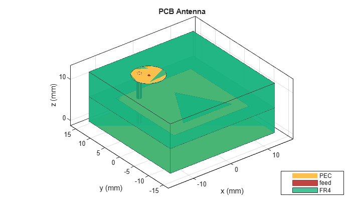
Visualize the PCB antenna.
figure
show(pcbAnt)
title("PCB Antenna")