Hardware Implementation Pane
R2026bHardware Implementation Pane Overview
Configure hardware parameters for an FPGA or SoC device when using the SoC modeling and generation feature set. These parameters enable code generation for rate-based and event-based tasks. They also enable advanced profiling capabilities, such as task and core profiling, and code and kernel instrumentation. To configure these parameters, follow these steps:
On the Simulink® toolstrip, on the Modeling tab, click Model Settings.
In the Configuration Parameter dialog box, click Hardware Implementation.
Set the Hardware board parameter to
Altera Arria 10 SoC development kit,Altera Cyclone V SoC development kit, orArrow SoCKit development board.Then, click Apply.
If you chose
Altera Arria 10 SoC development kitorAltera Cyclone V SoC development kit, set Feature set for selected hardware board to SoC Modeling and Generation and click Apply.The parameter values under Hardware board settings are automatically populated to their default values. You can optionally adjust these parameters for your particular use case.
Click Apply.
If you want to enable code generation for rate-based tasks and basic profiling capabilities, set Feature set for selected hardware board to Embedded Coder. For information about configuring the associated hardware parameters, see Hardware Implementation Pane: Arria 10, Cyclone V, or Arrow SoCKit.
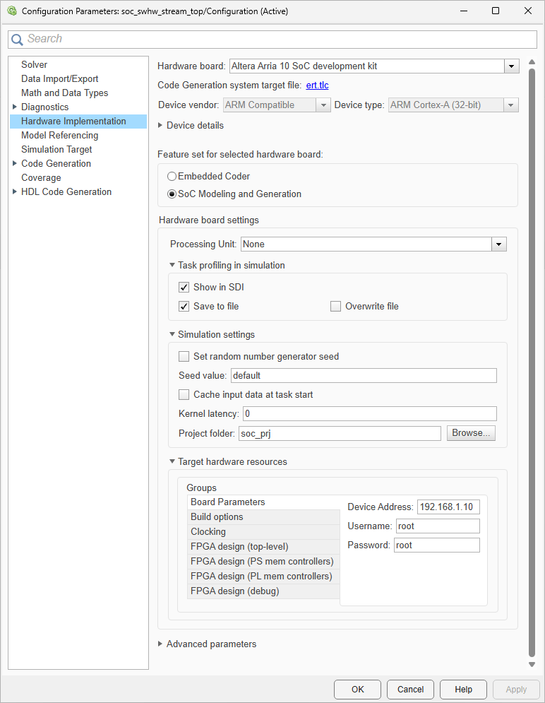
Hardware board settings
Set the processing unit to build and deploy the application model.
| Parameter | Description | Default Value |
|---|---|---|
| Processing Unit (SoC Blockset) | Select processing unit for SoC model deployment. | None |
Task profiling in simulation
Define the settings to display and record tasks in simulation.
| Parameter | Description | Default Value |
|---|---|---|
| Show in SDI (SoC Blockset) | Show the task execution data collected in simulation in the Simulation Data Inspector application. | on |
| Save to file (SoC Blockset) | Save the task execution data to a file. | on |
| Overwrite file (SoC Blockset) | Overwrite the last task execution data file. | off |
Task profiling on processor
Define the settings to display and record tasks on hardware board.
| Parameter | Description | Default Value |
|---|---|---|
| Show in SDI (SoC Blockset) | Show the task execution data collected on hardware in the Simulation Data Inspector application. | off |
| Save to file (SoC Blockset) | Save the task execution data to a file. | off |
| Overwrite file (SoC Blockset) | Overwrite the last task execution data file. | off |
| Instrumentation (SoC Blockset) | Choose to perform code instrumentation or Kernel instrumentation. | Code |
| Profiling duration (SoC Blockset) | Choose whether to perform Kernel profiling for an unlimited or limited time duration. | Unlimited |
Operating system/scheduler
Define the kernel latency of the OS in simulation of a task.
| Parameter | Description | Default Value |
|---|---|---|
| Operating system (SoC Blockset) | Specify the operation system. |
|
Simulation settings
Define the settings used to simulate task execution timing.
| Parameter | Description | Default Value |
|---|---|---|
| Set random number generator seed (SoC Blockset) | Set the random number generator seed. | off |
| Seed Value (SoC Blockset) | Specify the seed value for the simulation of task duration deviation. |
|
| Cache input data at task start (SoC Blockset) | Cache the input data at the start of a task. |
|
| Kernel latency (SoC Blockset) | Set the simulated delay. |
|
| Project folder (SoC Blockset) | Specify the project folder. |
|
Board parameters
Define the board parameters.
| Parameter | Description | Default Value |
|---|---|---|
| Device Address (SoC Blockset) | Network address of hardware board or device. | 192.168.1.10 |
| Username (SoC Blockset) | Login username on hardware board or
device. |
|
| Password (SoC Blockset) | Login password on hardware board or device. |
|
Processor
Specify processor features for the entire model.
| Parameter | Description | Default Value |
|---|---|---|
| Number of cores (SoC Blockset) | Set the number of CPU cores in the processor. | 1 |
Build options
Define how SoC builder tool responds when you press
Ctrl+B to build your model.
| Parameter | Description | Default Value |
|---|---|---|
| Build Action (SoC Blockset) | Defines how SoC Builder tool responds when you build your model. | Build, load, and run |
Clocking
Define the settings for the clock signals on the embedded processor.
| Parameter | Description | Default Value |
|---|---|---|
| CPU Clock (MHz) (SoC Blockset) | The CPU clock frequency in MHz. | 1000 |
External mode
Define the external mode communication properties of a model.
| Parameter | Description | Default Value |
|---|---|---|
| Communication Interface (SoC Blockset) | Transport layer used to exchange data between the development computer and hardware. |
|
| Run external mode in a background thread (SoC Blockset) | Execute the external mode engine in the generated code in a background task. |
|
| Port (SoC Blockset) | IP address port on hardware board. | 17725 |
| Verbose (SoC Blockset) | Enable view of the external mode execution progress and updates in the Diagnostic Viewer. |
|
FPGA design (top-level)
Define the FPGA design parameters for the entire model.
| Parameter | Description | Default Value |
|---|---|---|
| Include AXI Manager IP for host-based interaction (SoC Blockset) | Use host-based scripts with an integrated JTAG manager on the target platform. |
|
| Include processing system (SoC Blockset) | For processor-based platforms, include the processing system. |
|
| Register configuration clock frequency (MHz) (SoC Blockset) | The system configuration clock drives the configuration register interfaces for the vendor IP cores in the system. |
|
| IP core clock frequency (MHz) (SoC Blockset) | The clock for all Simulink based generated HDL IP cores. |
|
FPGA design (PS mem controllers)
Define the FPGA design parameters for the PS memory controllers. The default values for these parameters vary by board.
| Parameter | Description | Default Value |
|---|---|---|
| Controller clock frequency (MHz) (SoC Blockset) | Frequency of datapath between PS memory interconnect and PS memory controller. |
|
| Controller data width (bits) (SoC Blockset) | Bit width of datapath between PS memory interconnect and PS memory controller. |
|
| Bandwidth derating (%) (SoC Blockset) | For every 100 clocks, will hold off all transaction execution for this number of clocks. |
|
| First write transfer latency (clocks) (SoC Blockset) | Number of clock cycles between write request and start of transfer. |
|
| Last write transfer latency (clocks) (SoC Blockset) | Number of clock cycles between the end of write transfer and completion of transaction. |
|
| First read transfer latency (clocks) (SoC Blockset) | Number of clock cycles between read request and start of transfer. |
|
| Last read transfer latency (clocks) (SoC Blockset) | Number of clock cycles between the end of read transfer and completion of transaction. |
|
FPGA design (PL mem controllers)
Define the FPGA design parameters for the PL memory controllers. The default values for these parameters vary by board.
| Parameter | Description | Default Value |
|---|---|---|
| Controller clock frequency (MHz) (SoC Blockset) | Frequency of datapath between PL memory interconnect and PL memory controller. |
|
| Controller data width (bits) (SoC Blockset) | Bit width of datapath between PL memory interconnect and PL memory controller. |
|
| Bandwidth derating (%) (SoC Blockset) | For every 100 clocks, will hold off all transaction execution for this number of clocks. |
|
| First write transfer latency (clocks) (SoC Blockset) | Number of clock cycles between write request and start of transfer. |
|
| Last write transfer latency (clocks) (SoC Blockset) | Number of clock cycles between the end of write transfer and completion of transaction. |
|
| First read transfer latency (clocks) (SoC Blockset) | Number of clock cycles between read request and start of transfer. |
|
| Last read transfer latency (clocks) (SoC Blockset) | Number of clock cycles between the end of read transfer and completion of transaction. |
|
FPGA design (debug)
Define the FPGA design parameters for debugging.
| Parameter | Description | Default Value |
|---|---|---|
| Include AXI interconnect monitor (SoC Blockset) | Gather performance metrics of the memory interconnect such as data throughput, latency, and number of bursts executed. |
|
| Trace capture depth (SoC Blockset) | Maximum number of Trace entries to be logged in trace mode |
|

