CPFSK Modulator Baseband
Modulate using continuous phase frequency shift keying method
Libraries:
Communications Toolbox /
Modulation /
Digital Baseband Modulation /
CPM
Description
The CPFSK Modulator Baseband block modulates a signal using the continuous phase frequency shift keying (CPFSK) method. The output is a baseband representation of the modulated signal. For more information about the modulation and the filtering applied, see Algorithms.
Examples
Demodulate a CPFSK-modulated signal impaired by AWGN and compute the bit error rate.
The cm_cpfsk_mod_demod model generates random integer data, converts it to bipolar values, and then applies CPFSK modulation to frames data. The CPFSK-modulated signal passes through an AWGN channel and then is demodulated by using the CPFSK method. The bit error rate is calculated on frames of data.
The Error Rate Calculation block has the receive delay set to the value of the traceback depth used by the CPFSK Baseband Demodulator block. The model uses the Find Delay block to confirm the delay equals the value of the traceback depth.
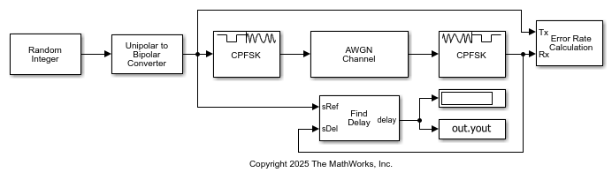
Transmit to receive delay is 16 symbols.
BER = 0.0033255
Nonlinear digital demodulation techniques can be more prone to issues caused by misalignment of symbol boundaries due to their sensitivity to timing errors, increased susceptibility to intersymbol interference (ISI), and potential for introducing nonlinear distortions. For the demodulation to work correctly, the input signal to the demodulator block must have the correct alignment. Various blocks between the modulator and the demodulator introduce processing delays, leading to incorrect alignment. This example shows how to correct this type of misalignment.
Open the Model
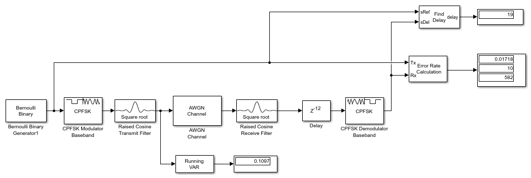
The model includes the following blocks:
The Bernoulli Binary Generator block generates random binary inputs.
The CPFSK Modulator Baseband and CPFSK Demodulator Baseband blocks use continuous phase frequency shift keying (CFPSK) for modulation and demodulation.
The Raised Cosine Transmit Filter and Raised Cosine Receive Filter blocks to apply pulse shaping by interpolating and decimating the input signal using a raised cosine finite impulse response (FIT) filter.
The AWGN Channel block is for channel modeling.
The Error Rate Calculation block computes the bit error rate.
Adjust Delays
The CPFSK Demodulator block processes each collection of eight samples per symbol to compute one output symbol. For binary CPFSK with a modulation index of 1/2, the demodulator input must align along even numbers of symbols. The requirement applies only to binary CPFSK with a modulation index of 1/2. Other CPM schemes with different M-ary values and modulation indexes have different requirements.
Both the Raised Cosine Transmit Filter and the Raised Cosine Receive Filter introduce a group delay (GD) in the system. Set the Filter Span in Symbols property in both the filters to 2*2 . GD in symbols is half of the filter span which is 2 , and the combined GD is 4.


To ensure that the CPFSK Demodulator block receives the input samples in aligned to the start of the traceback depth specified in the block, you use the Delay block to introduce a delay of 12 samples. In sample-based mode, the CPFSK Demodulator block introduces a delay of Traceback length + 1 samples at its output. With a Traceback length of 16, the total CPFSK Demodulator Delay is 17 and the total receiver delay is 17 + 2 = 19 samples.
Run the Model
When you run the model, you can see:
Evaluate Error Rates
The Error Rate Calculation block shows a minimal error count, indicating an overall low error rate in the system compared to the number of samples evaluated. This outcome results from the absence of alignment issues, ensuring high data integrity and system performance.
To establish a baseline, remove the noise from the system by deleting the AWGN Channel block from the model. The Error Rate Calculation block then reports zero errors.
Observe Effects of Misalignment
In the model, remove the delay block. The demodulator input does not align along even numbers of symbols. Consequently, this misalignment leads to a significant increase in the error rate and the number of errors reported by the Error Rate Calculation block.
Conclusion
Managing delays and alignment ensures data integrity and system performance. By incorporating a delay block to compensate for the misalignment caused by the Raised Cosine Transmit and Receive Filter blocks, you can see that the model successfully aligns the symbol boundaries before the demodulation process and reduces the overall error rates.
Ports
Input
Output
Parameters
Block Characteristics
Data Types |
|
Multidimensional Signals |
|
Variable-Size Signals |
|
More About
Algorithms
References
[1] Anderson, John B., Tor Aulin, and Carl-Erik Sundberg. Digital Phase Modulation. New York: Plenum Press, 1986.
[2] Proakis, John G. Digital Communications. 5th ed. New York: McGraw Hill, 2007.
Extended Capabilities
Version History
Introduced before R2006a