Random Access of External Memory Using Altera Devices
R2026bThis example shows how to model external memory accesses from an FPGA for rotating an ASCII art image. Many applications require the FPGA to access memory in a random fashion as per the requirements of algorithm. You learn how to design memory address generation along with other AXI4 master signals to read and write specific regions of memory. You simulate, implement, and verify your design on hardware.
Supported hardware platforms:
Altera® Arria® 10 SoC development kit
Altera Cyclone® V SoC development kit
Design Task
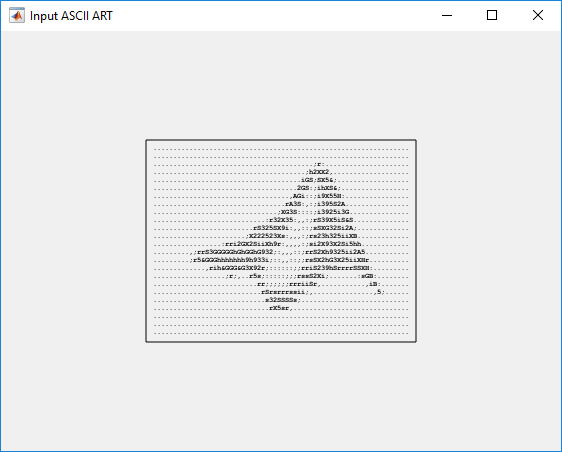
The ASCII art image is encoded as 24-by-64 matrix of uint8 characters. The design task is to rotate the image by modeling AXI4 Master interfaces in FPGA logic for external memory access. By simulating the design with external memory model and the AXI4 protocol, you verify the behavior at application design time. This saves time otherwise spent in debugging the design on hardware during the implementation phase.
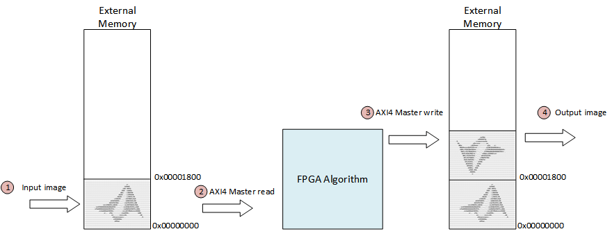
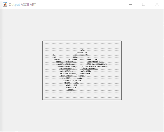
The overall dataflow is as described in figure below. The image is stored in the external memory at the memory region from address 0x00000000 to 0x000017FF. FPGA algorithm reads the image from this region and rotates it by writing it in the reverse order into the memory region from 0x00001800 to 0x00002FFF. Finally, the data is read back from the memory.
Model Structure
The models are structured using model references. Top model ' alterasoc_image_rotation ' includes the FPGA model ' alterasoc_image_rotation_fpga ' using model block as model reference.
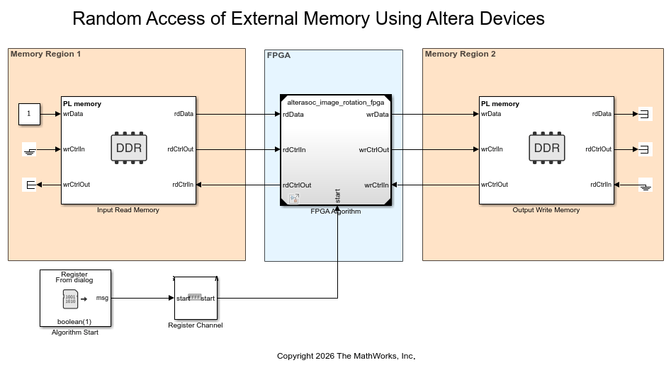
The top model covers the following areas:
Memory Region 1: The Input Read Memory block models memory region 1 using an AXI4 Random Access Memory block. The Input Read Memory block stores the input image and initializes the memory before the simulation starts. To see how model parameters and input data are initialized, open the preload simulation function <matlab:edit('alterasoc_image_rotation_init').
FPGA: This area instantiates the FPGA model reference, which models the logic for AXI4 Master interfaces and data rotation.
Memory Region 2: The Output Write Memory block models memory region 2 using an AXI4 Random Access Memory block. The Output Write Memory block stores the rotated image and logs it at the end of the simulation. To see how the input and output data are plotted, open the stop simulation function soc_image_rotation_post.m.
Control: The
Algorithm Startblock sends astartsignal to the FPGA algorithm via the Register Channel block.
The FPGA model implements the algorithm in three subsystems: AXI4MasterRead, ReverseDataOrder, and AXI4MasterWrite. Open the FPGA subsystem for image rotation:
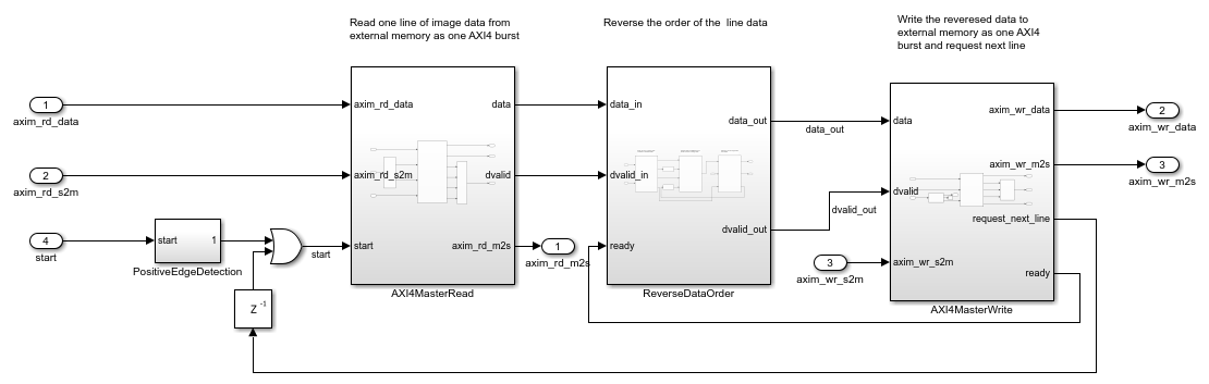
As the positive edge of the start signal is detected, AXIMasterRead reads one line of image data and delivers it to ReverseDataOrder to reverse the order of data. The reversed data is then written to external memory by the AXIMasterWrite subsystem. After one line of data is written, it sends a request_next_line signal to trigger the reading of the next line by AXIMasterRead. This cycle continues until all lines of the image are processed.
Open AXI4MasterReadController and AXI4MasterWriteController blocks to inspect the MATLAB® code for the AXI4 Master interfaces. These blocks design the addressing logic for read and write operations as per the AXI4 protocol. AXI4 Master protocol and for timing diagrams of AXI4 signals, see Model Design for AXI4 Master Interface Generation.
Simulation
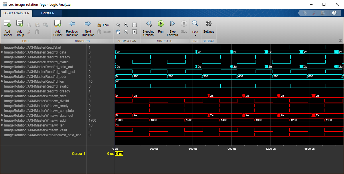
Run the model and open the Logic Analyzer from the FPGA model. Notice the following key points:
One line of data is written or read by masters in one burst. Since each line is 64 characters long; the burst length is 64 (0x40). Note this value on the
rd_lenandwr_lensignals.Each character has 4 bytes as it is extended to uint32 data type, which makes the length of line 64x4 = 256 (0x100) bytes. Therefore, addresses increment or decrement by 0x100. Note this on the
rd_addrandwr_addrsignals.One read burst is followed by one write burst. Observe how
rd_dvalidandwr_dvalidtoggle alternatively.request_next_lineasserts after each write burst, which triggers the next read burst.
The input and output images are plotted at the end of the simulation.
Implementation
To implement the model on a supported FPGA board, use the SoC Builder (SoC Blockset) tool. Set Hardware Board to Altera Arria 10 SoC development kit in the top model. Make sure you have installed the required products and FPGA vendor software before implementation.
Open SoC Builder by clicking Configure, Build, & Deploy button in the toolstrip and follow these steps:
Select Build Model on Setup screen. Click Next.
Click View/Edit Memory Map to view the memory map on Review Memory Map screen. Notice that the base address 0x80000000 is assigned to Input Read Memory block, and base address 0x80002000 is assigned to Output Write Memory block. The AXI4 address is the sum of the base address and the address from FPGA algorithm. For example the output data is written to the external memory from address 0x80002000 to address 0x80002000 + 0x17FF = 0x800037FF. Refer to Model Design for AXI4 Master Interface Generation for more information about base address register calculation. Click 'Next'.
Specify project folder on Select Project Folder screen. Click Next.
Select Build, load and run on Select Build Action screen. Click Next.
Click Validate to check the compatibility of model for implementation on Validate Model screen. Click Next.
Click Build to begin building of the model on Build Model screen. An external shell will open when FPGA synthesis begins. Click Next to Load Bitstream screen.
The FPGA synthesis can take more than 30 minutes to complete. To save time, you can use the provided pre-generated bitstream by following these steps:
Close the external shell to terminate synthesis.
Copy pre-generated bitstream to your project folder by running the command below and then,
Click Load button to load pre-generated bitstream.
copyfile(fullfile(matlabshared.supportpkg.getSupportPackageRoot,'toolbox','soc','supportpackages','intelsoc','intelsocexamples','bitstreams','alterasoc_image_rotation-a10soc.sof'), './soc_prj');
To run this example, copy the example testbench to your project folder.
copyfile(fullfile(matlabroot,'toolbox','soc','supportpackages','intelsoc','intelsocexamples','alterasoc_image_rotation_aximanager.m'), './soc_prj','f');
Enter the following command to run the testbench:
alterasoc_image_rotation_aximanager
The testbench performs the following operations:
Initializes the image rotation IP
Writes the input image data to external memory
Starts the image rotation operation
Reads back and displays the output image data from external memory
If you want to target a different FPGA board, you need to apply the following settings in the configuration parameters of the top model before launching the SoC Builder.
Select the Hardware board under Hardware Implementation panel to match your board.
Clear Include processing system under Hardware Implementation -> Target hardware resources -> FPGA design (top-level) panel.
Note that the pre-generated bitstream may not work if you customized the memory map.
Conclusion
This example shows the modeling of AXI4 Master interfaces for accessing external memory in a random fashion by rotating an ASCII art image. You can use this as a guide to design your own algorithm to access memory directly using the AXI4 Master protocol.

