Modeling and Simulating Otava mmWave Beamformer IC - MATLAB & Simulink
Video Player is loading.
Current Time 0:00
Duration 46:11
Loaded: 0.36%
Stream Type LIVE
Remaining Time 46:11
 
1x
  • descriptions off, selected
  • en (Main), selected
    Video length is 46:11

    Modeling and Simulating Otava mmWave Beamformer IC

    Overview

    Learn about modeling and simulating the single chip Otava beamformer IC (BFIC), a wideband 8-channel transmitter and receiver operating at mmWave frequencies.

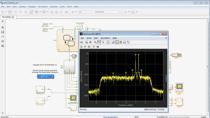
    Based on actual measurements, this Simulink model allows verifying and optimizing the system performance in different operating conditions while taking into account the impact of impedance mismatches, antenna arrays, and non-linearity. Circuit envelope RF simulation and testbenches will allow you to integrate the BFIC into wideband communications systems, including modulated waveforms and phased array beamforming algorithms. Using this model - representing the executable specifications of the BFIC - you’ll be able to calibrate the system and rapidly develop 5G, SATCOM, and DoD applications.

    Highlights

    • Using the Otava mmWave beamformer IC together with Xilinx RFSoC
    • Developing beamforming 5G, SATCOM, and DoD applications
    • Using the model as an executable specification of the IC
    • Integration of the BFIC together with full TX and RX signal chains and different antenna arrays

    About the Presenters

    Cecile Masse - Otava Inc.

    Cecile Masse is a senior RF systems architect, based in Orange County, California. She has more than twenty years of experience in the wireless and semiconductor industry. Cecile has held a number of roles with responsibilities ranging from radio design to IC products specification, system modeling and optimization, customer engagement, project management and technical training. Working for large corporations such as Analog Devices, as well as start-up companies, she has defined numerous RF and mixed-signal products. She has also developed successful reference designs and development platforms for multi-carrier GSM, 3G, 4G LTE and more recently for millimeter wave 5GNR. The core of her expertise lies in wideband, high performance radio design. She holds a Master’s degree in Electrical Engineering from the engineering college E.S.I.E.E, Paris, with majors in RF design and signal processing.

    Giorgia Zucchelli - MathWorks

    Giorgia Zucchelli is the product manager for RF and mixed-signal at MathWorks. Before moving to this role in 2013, she was an application engineer focusing on signal processing and communications systems and specializing in analog simulation. Before joining MathWorks in 2009, Giorgia worked at NXP Semiconductors on mixed-signal verification methodologies and at Philips Research developing system-level models for innovative communications systems. Giorgia has a master’s degree in electrical engineering and a doctorate in electronics for telecommunications from the University of Bologna.

    Recorded: 29 Mar 2022

    Hello, and welcome to this MathWorks webinar. Today we're going to cover a very interesting topic. We are going to see how to model and simulate Otava millimeter wave Beamformer Integrated Circuit. or how we call it affectionately, the BFIC.

    My name is Georgia Zucchelli. I've been with MathWorks for over a decade. I initially started as an application engineer, and then around 2013 I transitioned to a more focused role as product manager. A long time ago before MathWorks, I worked for NXP Semiconductors and Philips Research, where I also modeled innovative wireless communication systems such as the one that we are going to see today.

    And today together with me, I would like to very warmly welcome a very special guest, Cecile Masse, RF system architect from Otava. Welcome Cecile, and thank you very much for joining us. Before we get started and I pass the ball to Cecile, who will tell us all about the BFIC and the models that we developed, let's see a little bit more details what we are going to cover today.

    We will start by introducing Otava Beamformer IC, the BFIC. We will describe why and how we created this MATLAB based model. So we we'll definitely cover the model structures, and also how we embedded the characterization data in the model. We will also describe how to integrate these models within a larger system-- so how to integrate it with antenna arrays for transmitter receiver, for the development of verification of beamforming systems, and also how to integrate it with streaming signals such as OFDM signal.

    We will use demos, showing the model in action. And then we will summarize with conclusions, next steps, and give you the opportunity to ask questions, of course. But before we start, let me pass it over to Cecile. Welcome, Cecile. Can you please tell us a little bit more about yourself, Otava, and the BFIC?

    Thank you, Georgia. Hi, everyone. My name is Cecile Masse, and I've been an RF and wireless system engineer for many years, working for large and small companies, manufacturing integrated circuits as well as subsystems. I've started my career working on kilohertz GSM radios, and now keeping up with bandwidth expansions of unlimited applications of 5GNR systems.

    So back in 2021-- early 2021-- Otava Incorporated, which is a startup company based in New Jersey, introduced their wideband Beamformer IC, shown on the bottom left here, along with other millimeter wave products following this one over the next few months. And it was targeted at FR2 bands. And as a way to speed up the evaluation and optimizations of phase array systems, with this Beamformer IC, we partnered with MathWorks to create an accurate behavioral model for it. This really was a way to help radio designers in their system-level design before the actual hardware implementations.

    So let me begin going over some detail about this particular device. The Otava Beamformer IC, which is called OTBF103, is a fully integrated eight-channel transmit and receive from a circuit, that's meant to interface to a phased array system and operate in the FR2 bands between 24 and 40 gigahertz. It is designed to interface directly to a millimeter wave transceiver on one end and a phased array antenna on the other, with or without external components.

    Eight received channels take the signal from the antenna elements, and are combined to a common RF ports to be demodulated. And the reverse is done on a transmit, where the millimeter wave signal from a transceiver gets converted and split into eight independent channels. All these channels integrate gain control amplifier with 20 dB range, as well as independent phase control over 360 degrees.

    This Beamformer IC also integrates temp sensors, RMS power detectors, as well as gate drivers for external amplifiers, and also switch drivers for an external T/R switch. All these channels, whether transmit or receive, are digitally controlled through a high speed SPI interface.

    So here's a top-level view of a full array radio unit from the digital basement block on the left, that processes the uplink and downlink streams from the users in the cell, to the millimeter wave modulator and then to the RF front-end circuits, where the millimeter wave signals are multiplexed over a number of analog channels, driving the antenna element of the subarray. This is where the BFIC that we'll be talking about sits in the chain. And to drive these millimeter wave front-end circuits, Otava has also been working closely with Avnet to build subsystem modules and reference design based on the Xilinx RFSoC products, as illustrated at the bottom of this slide.

    As I mentioned earlier the OTBV103 covers a fairly wide range of RF frequencies, between 24 and 40-- so over 16 gigahertz. It may be used for a wide range of 5G NR systems. And the bandwidths are highlighted here in blue. But it is also applicable for certain satcom systems as well as defense systems.

    So not only RF designers can get their hands on the Beamformer eval board here, but they can also get started now with a MATLAB model if that's the preferred step. The beamformer model is broken down in two separate sub-blocks, so one for the transmit channels and one for the receive ones. These models go beyond the traditional S-parameter files, and are a very useful complement to the eval board PCBs.

    So system design designers and RF designers may get started with the MATLAB model first, especially when experimenting with various antenna configurations. Plus, it helps get started-- a head start on the design, both hardware and software, before all the pieces of the radio system can actually be put together. So before we started, we had to define a set of goals and capabilities for this particular model. There's a lot in there, and the key questions were, what is this supposed to do, and what should RF designers and system designers be able to accomplish with it?

    So we've built this model in MATLAB Simulink, taking advantage of the RF blockset envelope simulation capabilities. It was really built to enable bits to antenna system level simulation, RF signal chain optimization, all the way to even algorithm development. So it was really built with that mindset of helping users build their antenna radio system, and help with radio design in general.

    So the performance that we wanted to capture needed to be representative of the circuits over a number of parameters. RF frequency of operation, for sure, that's the first one. But also, what gain setting of the gain control amplifier, as well as the phase shifter setting for all the individual channels. And of course, how the device would perform over various input power level or output power level.

    So something I would like to highlight here, which is quite important-- we spent quite a bit of time on this-- is really, that we wanted this model to be based on actual measured data. So it will capture RF performance over all these parameters. But as far as like even residual amplitude and phase error, as a function of the operating point.

    So here's a first view of the guts of the model, and Georgia will go over the modal structure shortly, more in detail. So it's been structured in a way that facilitates the integration of all these measured data and through-captures. This list of items basically has parameters for the input and output, that was a key goal important here.

    Gain versus frequency. Compression points such as P1dB and IP3 as a function of various states of the BFIC gain stating and frequency. But also noise figure, amplitude error, phase error, as a function of phase and gain state. Also there's quite a bit of capabilities here that's been embedded in this model.

    And the user, when they're going to get started with the model, they're going to need to enter or even calculate the following parameters. Basically the standard frequency of operation, CF. Also the gain setting for each individual channel, and that could be the same for all channels. That could be a vector for calibration or tapering.

    And finally, the phase for individual channels, and that's an important parameter here that could also be a vector. And that will be useful when doing beam steering. So that is my introduction. And Georgia, going now back to you here, and how we put together this model and how it is structured.

    Thanks, Cecile. So when we developed the BFIC models, the first modeling guideline that we wanted to follow was to separate the device under test from the test bench or the test benches. This is really a guideline that pretty much is followed any time that you develop software, but it's very valid also for modeling approaches.

    The other thing that we wanted to do is, to make sure that the device and the test of the BFIC model use the electrical interfaces. That's the interfaces in the domain of the voltage and the currents. Because we wanted to provide the ability to model impedances and impedance mismatches, which are very important at these operating frequencies. And we wanted to do this for both the transmitter and the receiver as well as the input and the output.

    For the device on the test, we wanted to provide the ability for the users to specify the configuration settings-- the operating frequency, the VGA code, and the phase shifts as Cecile described. And we wanted to have the behavior of the device under test to be driven by measurement data that is directly embedded inside the model. And the data is also suitably interpolated based on the configuration settings, so depending on which data is available from the measurement.

    For the testbench or the testbenches, we wanted to provide the ability for the users to change the stimulus and to perform different RF measurements, as well as to change some of the global parameters-- such as, for example, what is the best frequency. Or if you test the receiver, what is the direction of arrival of an incident plane wave.

    At the high level, the structure of the models for-- inside the models, let's say, inside the transmitter and receiver-- is very, very similar. So for the transmitter, the functional architecture is essentially made of four blocks. It starts with an eight-way splitter, that also captures the BFIC with impedance. It's followed by a programmable phase shifter.

    It's followed by a programmable amplifier, or a VGA for each of the elements of the chain, that provides the ability to model the residual phase and gain-- so the total cascaded gain plus phase error, so the full chain. And it's followed by an amplifier that captures the S-parameters for transmission, reverse isolation, and reflection, as well as the output referred the non-linearity for the transmitter.

    The receiver implements, essentially they reverse this structure. Also made of four blocks. At the input, we have an amplifier that models the input impedance of each element of the chain, as well as the noise characteristics and the input referred non-linearity, which is followed by the VGA programmable amplifier, programmable phase shifter, and then the outputs of each of the eight chains are strung together with an eight-way power combiner.

    One thing to keep in mind is that this structure doesn't really represent the architecture of the BFIC, but is a trade-off because it allows us to capture all the measured RF effects. And it also provides the maximum flexibility for the users to program both the transmitter and the receiver, and so to use the model in different operating conditions.

    In practice when you open the library, when you open the Simulink model of the transmitter BFIC, you can look at its underlying structure by just clicking the gray arrow that is in the bottom left corner. And you can recognize the four elements of the network that we just discussed. If you double click on the component, you will open up its mask where you can provide the user defined parameters for the operating center frequency between 24 and 40 gigahertz, the VGA codes-- there can be an array or a scalar-- and the phase shifts, that they can also be an array or a scalar. And then both the VGA codes and the phase shift can be used to implement-- regain calibration in beamforming.

    Also in the mask, you can see the quantized values for the applied phase shifts that are used effectively by the BFIC. And this is particularly helpful when you test this component in the lab. Last but not least, also from the mask of the block, you can plot the characteristics of the BFIC at a given operating frequency. So you can see gain or quantity compression point. For example, noise figure center at the center frequency as well as the S-parameters.

    The nominal operating conditions are computed using a static analysis, and they're directly derived from the I/O measurements data that is embedded inside the model. So this gives you an indication of how the device behaves at a given frequency. For the receiver, the concept is very, very similar.

    You can open the Simulink model, you can click on the gray arrow on the bottom left corner, and look underneath how it is implemented. again, the four elements are cascaded together to represent the behavior and the programmability of the behavior. If you double click on the component, you open up its mask with user-defined parameters-- just like we said before, center frequency, VGA codes, and phase shifts. And again, you can plot the characteristics of the receiver at a given operating frequency.

    So you can look at its P1dB, IP3, noise figure at a center frequency, as well as the S-parameters. This is very convenient because essentially, you can really verify immediately in a matter of seconds, which operating range you are making the model work. Now back to you, Cecile, to describe a little bit more in detail the capabilities of these models, and how the users can actually use them.

    Well, the first testbench of interest when you get started with the BFIC model, are the RF measurement testbench. And here's the one we have for transmit channel simulation, built around the transmit BFIC model here at the bottom. They are meant for single channel as well as multichannel simulation. And you could also use external circuitry like a millimeter wave upconverter, or your own custom source as well.

    Here's the receive testbench. It's built really in a similar fashion around the beamformer receive model. And they're structured the same way with three selectable RF measurement blocks.

    The first one allows for gain, IP3, noise figure simulation. That's shown on the top. The second one is for S-parameter extraction, and an example of what you would get on when you run the simulation here. And finally the last blocks in this testbench allows for modulated waveform analysis such as ACLR and EDM.

    In each case, the user will need to specify the operating frequency and the global parameter box here at the top of the testbench, as well as the BFIC gain setting, which is gain code between 0 and 255. That will correspond to attenuation level between the minus 20 and 0 dB. I would like to point out that the model has been checked again the initial set of measured data.

    So this example on the right, which shows IP3 performance or simulated IP3 performance, matches the measured level within a few tenths of a dB. Here with the same testbench, we have simulated DRF performance with a modulated waveform. As you can see, the testbench will return a ACLR measurement as well as RMS output power level with this first spectrum plot here on the center. But it'll also display the constellation, so you can see the 64 QAM constellation here along with the equivalent RMS EVM measurements. So it is quite handy and quite useful for our designers.

    The default waveform used here is 100 megahertz OFDM signal with random bitstream. And users may change the input drive level to the BFIC, the output power. They also could potentially also change the waveform in itself-- the better structure that way. And I also want to point out that you don't have to worry about the instantaneous phase through each of these channels. So no matter what the phase setting is through the BFIC, the demodulator embedded in these OFDM testbenches will take care of the phase and frequency recovered.

    There is an additional testbench for the received BFIC, and that's really meant to quantify the total system gain as a function of a number of active channels. So this is using this parametric source block here on the left, where you can play with the number of active or inactive channels, and extract the total end-to-end gain. So for instance, if you have two channels, you only get plus 6 dB gain. And three channels, you get plus 9 and a half, et cetera.

    But you can also use it to extract SNR measurement as shown on this example, and with this spectrum plot. Here we measured SNR about 108.5 per kilohertz with all the channels on, or 138 dB per hertz. And we used this number to calculate an equivalent noise figure per channel based on the signal channel gain.

    So in this case, we're backed off at 3 dB. We've got a gain of 13.3, and we extract noise figure 4.6, which turns out to be quite close to the actual measured value of 4.4. So quite nicely matches what you would expect out of the actual device.

    A very important aspect of radio design-- and this is really the key goal of building this l-- is for phased array, front-end design, and the analysis of the interaction between the antenna alignment and the active circuit that interfaces with it. So these front-end subsystems are not necessarily trivial to design. And interactions between the beamformer IC and the antenna elements is something you want to get a good understanding fairly early on, especially when it comes to over-the-air performance, passed in response of the main beam, side lobe rejection, grating lobes, and pattern nodes even.

    So this is where we spent a bit of time in there, to put together this starter testbench with the BFIC model attached to it. Not only you'll be able to plot the transmitted radiation pattern, as shown here on the right as a function of the desired beam direction-- so here, showing this example for 10 degree beam steering angle. But also we're reporting EIRP-- Effective Isotropic Radiated Power, which is quite an important design parameter when you look at a transmit array. It is extracted based on both the electrical and magnetic field in the far field regions, assuming 100 lambda distance. It also accounts for the calculated element directivity for the antenna element.

    And now inside the antenna model mask, we can see how the eight transmit ports of the beamformer IC are attached to the antenna model, shown by this mask here. This is capturing the element impedance for the array object here, which is an eight-element dipole. And it's been tuned about 30, 31 gigahertz here in this example, so you can see the return loss, that you can also plot with this testbench.

    And the eight by eight S-parameter of the design antenna array loads the BFIC circuit models. And the calculated RF output power level that shows on the upper right here, will actually take into account the element's impedance. Users can also access signal amplitude and the phase per element as a function of the desired steering angle.

    Finally, this is basically the equivalent-- beamformer receiver testbench for phased array analysis and receiver configuration. It's structured very similarly to the transmit one with the antenna elements. And the antenna array are defined with this mask here, that will compute the S-parameter and the directivity as a function of operating frequency. So every time you change the center frequency of operation here within the global parameter box, it will re-compute the array-- retune the array accordingly.

    An interesting feature we've added here, is that we have the ability to set certain feed loss between the antenna element and the beamformer IC. That could be a scalar-- like same value for all channel, or that could be something different for every individual channel. So right now it's a pure passive component.

    The source is a fixed CW source equivalent, and it will generate a fee current at the antenna elements from the far field plane wave. And it will do that, also accounting for a certain direction of arrival. This testbench right now assumes that the beamformer IC is set in the same direction of that incoming plane wave. And when you run the simulation, you'll be able to see output power as a function of the steering angle that's specified in the top level. So Georgia, why don't you show us some simulations of these testbenches?

    Absolutely, let's see the model in action. So let's go to MATLAB. And when you open the installation folder after you install the model, you will see three Simulink libraries-- the Otava library and two sub-libraries, the BFIC models and the testbenches. But the more conveniently after installation, if you open the Simulink Library browser, you will find the Otava library as well as the BFIC sub-library with the transmitter and the receiver ready for instantiation. And as well, the sub-library with all the testbenches-- some of them that Cecile described.

    Recommend you to start from here. And in this case, we will first open the receiver testbench. On the bottom you see the instantiated BFIC model. If we double click on it, then we open its mask. We can see the operating frequency indicated by the variable CF, in this case at 230 gigahertz. The VGA code of 180, that corresponds to 3 dB of automation, and is shown on the mask of the BFIC. And zero phase shifts because in this case, we're only testing the first channel.

    You can change the VGA code. For example, we can set it to 255. Or we can specify an array of VGA codes and papers. And as we change the value, we will see that the BFIC mask is updated with applied attenuation for each of the channels. But in this case, let's stay with 3 dB default attenuation just for convenience.

    At the bottom of the mask, we can plot the device nominal operating specification-- P1dB, IP3, noise filter, and the center frequency. That is in this case 30 gigahertz. And we can also see the S-parameters.

    Like we said before, this visualization is based on static analysis of the interpolated measurements that is embedded inside of the BFIC model. Let's try, for example, to change the center frequency. For example, we can change it to 24 gigahertz. As soon as we change it, we can replot the characteristics and verify once again how the receiver is working.

    As described before, we can click on the gray arrow on the bottom left corner of the model and we can inspect this underlying structure-- the four stages that we already described before, as well as essentially the phase and the amplitude phase shifts that are applied. We can now run the simulation. And for example, let's verify the gain of the first channel when tested using a CW tone at 30 gigahertz. And let's put the figure next to it, so we can compare the simulation results with the expected nominal volume. And we see that there is a good match with 13.3 dB approximately.

    And from the rough measurement unit, we can change the input power of this W tone. Or for example, we can measure the noise figure. That happens by integrating the output noise over the entire simulation boundaries. And in this case, you see that the measurement is settling towards 4.3 dB, and it is simulated in the time domain.

    Similarly, we can also measure the IP3 with two CW tones. And again, we can see that as the measurement settles, there is a little bit of limitation. Because the noise impacts at the intermodal product low in power. But as the measurement settles, we can see that there is a good match with expected results.

    Like I said before, from the same testbench you can also measure the S-parameters by using the second block in the testbench. Or you can test that the BFIC using a broadband OFDM signal to measure EVM and ACLR. This simulation is challenging because of the high operating frequency in the gigahertz range, as well as the large simulation bandwidth. We are talking about 100 megahertz and so forth.

    So to enable the RF simulation to BFIC device, we need to trade off the accuracy and the speed. And for this reason, we decided to use RF blockset circuit envelope simulation. This provides a good trade-off between the rear pass band modeling approach that is suitable for a transit simulation, but it is very slow. And the trade off between equivalent basement modeling approach, that is very fast but is only suitable for narrow band application.

    So circuit envelope provides also the advantage that enables multi-carrier stimulation for estimating the impact of nonlinear with interfering signals. And it enables time domain simulation for integration in larger systems. RF blockset, there is a lot that they can offer. With RF blockset, you can design the architecture and the specifications of your RF components, like it was done when designing the BFIC well before creating the models that we have presented today.

    You can integrate our front ends with adaptive algorithms such as DPD, AGC, beamforming. And later we will see how to integrate the BFIC with an antenna array for implementing beamforming. The benefit of an executable model is that you can test and debug the implementation of the transceiver before actually going to the lab, or before building prototypes.

    Or maybe while you are in the lab, you can do such a model to help you identify and test scenarios, or identify and debugging issues. Of course with the RF blockset, you can build models such as the one that we have seen today, also using and embedding directly measurements and data directly in your model. And you can share these models with your colleagues and your customers, just like Otava is doing today.

    And let's now go back to our testbench library and open the TX antenna testbench, or the transmitter antenna testbench. We find the BFIC connected to an antenna array, and on the top in pink, we have the ability to control the global parameters. If you open the mask of the transmitter antenna, we find the antenna object, the center frequency, and the direction of departure, as well as the ability to plot the far field radiation pattern. As soon as we plot it, the pattern is visualized, the directivity, and the EIRP.

    And we can also visualize additional antenna metrics. Notice that the power of the output signal on the testbench is also measured. And it's the same as the EIRP computed using electromagnetic analysis. And it also shows the additional distinction between the theta in the five polarization components.

    In this case, we use dipoles, and the power is aligned on the vertical direction. We can experiment a little bit more and change, for example, the angle of arrival-- 25 degrees. We can plot again the pattern. And indeed, we see that the beam gets tilted towards 25 degrees with updated directivity, EIRP, and antenna matrix.

    The beam is steered by the BFIC. You can see the phase shift here automatically computed based on the direction of departure. And we could also see the quantized values.

    But let's look a little bit more into the details of these array objects and how it is defined. It is defined in the matter of workspace. We can see that it is made of eight dipoles. We can visualize it by just using the show method, or we can analyze it-- for example, computing its pattern at 30 gigahertz. This is done using Antenna Toolbox.

    But an intuitive way to design your own array consists in using the Antenna Ray Designer app. Once you open the app, you can choose which type of array to design. In this case, we can use a linear array with, for example, eight elements. Once we design the array, we can choose the antenna type, and we have a very comprehensive catalog with different options. Can choose whatever we want in this case. Let's, for example, choose an array of monopoles.

    The next step, consists in designing the elements to make them resonant at the design frequency, 30 gigahertz, and also to be spaced by half wavelength. Now that we have designed the array, that the geometric properties are scaled, we can compute, for example, its pattern or we can compute its S-parameters using electromagnetic analysis. And of course we can iterate more with the design.

    Once we are happy, we can export this object to the MATLAB workspace. In this case, we export it with a different name. We call it new array. And another option for example, we can generate a script just to say something. Once we have the new array in the MATLAB workspace, again, we can visualize it. For example, we can analyze it as before. But more importantly, we can use it in our antenna block.

    So now we use the new array object in our antenna block. And then we can re-compute the pattern with updated directivity, EIRP, and antenna matrix. So you see how rapidly you can design a new array, or you can try out with different configurations-- including always the polarization effect.

    Let's see a little bit more in details how this antenna block works, because it's really interesting. So from the mask of the block, you can specify the antenna object. That is directly imported from the MATLAB workspace. And we have seen, for example, how to create this object using the app. But you can also create this object from the command line.

    You can specify if the antenna operates as a transmitter or receiver or both. And you can specify the center frequency of your signals. And actually I should say, the center frequencies-- because, for example, you could for a receiver, inject an out-of-band interfering signal. This is enabled by a circuit envelope that supports a Monte Carlo simulation.

    We can also specify the angle of direction, or the direction of arrival or departure. And last but not least, we can actually model both the S-parameters and the pattern over a frequency range, either using rational fitting, or a conversion-based approach. And this allows to take into account the effects of the tapering impedance and pattern over bandwidth when operating with wideband signals, which is very, very important.

    Behind the scenes, the transmitter and receiver antenna blocks allow you to model the effects of loading in terms of impedance, but also electrical coupling between the antenna elements. For example when we use patches, there is leakage in between the different elements. And this is done using the S-parameters. For the transmitter antenna block, the instantaneous voltage excitation applied at the terminal of the antenna is used to compute the far field radiation pattern, the directivity, and the EIRP.

    On the receiver side, the Simulink input signal actually represents an incident plane with excitation, and is used to compute the feed currents at the antenna terminals. When we use these blocks, the fundamental assumption essentially is that the transmitter and receiver spaced far apart, and there are no near-field effects between the two.

    One of the great benefits of this block is that the array impedance and the field are modeled over frequency. So we can take into account frequency-selective effects of the antennas. It takes into account the effect of polarization, both on the transmit side and on the receive side. This allows you to experiment with more complex scenarios. And essentially if something happens in between the transmitter and the receiver antenna, if you want to play around with the channel, you don't have to redo the electromagnetic analysis every time, which is very time-consuming.

    These blocks are enabled by Antenna Toolbox. Antenna Toolbox, like we've seen, have a catalog of antenna and array elements to rapidly get started, and offers the method of moments for accurate EM analysis. It offers a lot more. For example, you can do surrogate optimization or PCB design of cost of components, installation of antennas on platforms, as well as looking at RF propagation effects. So there is a wealth of capabilities in Antenna Toolbox.

    But enough for antennas right now. Now let's see how we can put all the tests mentioned that we have seen together. So let's look at a more comprehensive testbench. So let's go back to our library and open our OFDM testbench, where we can include both transmitter, the receiver, the antennas, beamforming, as well as streaming a wideband signal.

    Once we open the model, we see the testbench at the bottom. It provides the stimulus at minus 30 dBm at center frequency. The stimulus propagates through the BFIC transmitter. The transmitter array path loss of 70 dB, receiver antenna array, and the BFIC receiver. And then the testbench measures the results.

    When we run the simulation, as time progresses, the OFDM testbench measured the received spectrum on the left, and also recovers the transmitter constellation, as you can see it on the right. With the clock recovery mechanism, when it locks-- so you can see that the constellation is clean. And we can also compute the measure at EVM and CPR actually, on the spectrum analyzer on the left.

    Also on this testbench, like the ones that we've seen before, you can change the center frequency, the angle of departure and arrival, experiment with the entire link budget of your chain. And by the way, the global parameters are always indicated with the pink blocks.

    And starting from testbenches like this one, you can really experiment at your own pace with algorithms or your antenna components. And the bottom line is that you can really model the complete end-to-end chain. And without models such as this one, it's really hard to verify beamforming algorithms. And even if you've been in the lab, essentially, It's not easy to verify if you're really steering the beam towards a certain direction unless you have very sophisticated equipment. And sometimes it's essentially-- coming up with a prototype can be a large investment.

    With this, I'd like to summarize. So we have introduced the BFIC models. We've seen that they are based on actual measurement and they can reproduce the lab results before actually going to the lab. We showed testbenches that can be used for the performance verification of gain, IP3, noise figure, as well as S-parameter.

    We covered quite a little bit in detail how to integrate the BFIC models with the antenna arrays for beamforming applications. And we also showed how to use the full wave electromagnetic analysis to compute impedance, pattern, and polarization. And lastly, we just saw the testbench, and we saw how to enable the end-to-end simulation for system level integration. And really took advantage of the circuit envelope multi-carrier RF simulation both for high frequency and broadband applications.

    And you might wonder what's next. So to you, Cecile, what's next? What's the next steps for these models? There is already a lot, but what are the next steps?

    Yes, indeed, there is quite a bit covered already with these testbenches. So what else we could do here? Well, there's multiple things that could be done using these starting points. Build a 2D array, first combining multiple of these BFICs to build basically this N by M phase array system. So that would be the first thing beyond just a simple ULA.

    We could also insert a custom antenna module. And Georgia explained also how to use the app in MATLAB as well, to build your own. But that could also be coming from EM simulation files with S-parameter files, and your activity pattern that you can embed in using these, starting out as benches.

    And finally, you could also complete the whole signal chain around this BFIC model-- front-end circuit, and attach your own transceiver model using RF blockset, of course, or your own baseband source or RF signal or waveform source. That way you could also build this full transmitter receive system to extract link budget and signal quality. So there's quite a bit of advancement and future things that could be built around these starting blocks.

    Finally, now that we've concluded this presentation, if you want to get more information or get in touch with Otava, these are the links that you should write down. And an email address is also provided here. Thank you very much for your attention here. Georgia, you want to add more?

    Yes. If you want to learn more about the MathWorks tools that were used to develop these models, you can find a few reference links here for the RF blocks at circuit end of simulation, and Antenna Toolbox for the array analysis. And if you have any questions, please don't hesitate to reach out to me. I'm really looking forward to hear your questions. And I would like at last, to thank you very much again for your attention, and for staying with us today. And I hope to hear from you. Thank you.