pcbStack
Single feed or multi-feed PCB antenna
Description
The pcbStack object is a single feed or multi-feed printed
circuit board (PCB) antenna. Use the pcbStack object:
To create single-layer, multilayer metal, or metal-dielectric substrate antennas.
To create an arbitrary number of feeds and vias in an antenna.
To create a PCB antenna from antenna and array catalog elements.
Note
To generate a Gerber file, a substrate layer is required. Use the
Substrate property to create this layer in the PCB antenna.
For more information, see Convert Circular Microstrip Patch into PCB Antenna.
Creation
Description
pcbant = pcbStack
pcbant = pcbStack(PropertyName=Value)PropertyName is the property name
and Value is the corresponding value. For example,
pcbStack(FeedDiameter=2e-04) creates a PCB antenna
with a feed diameter of 0.2 mm. You can specify several name-value arguments
in any order as
PropertyName1=Value1,...,PropertyNameN=ValueN.
Properties that you do not specify retain their default values.
pcbant = pcbStack(ant)
Properties
Object Functions
array | Create array of PCB stack objects |
axialRatio | Calculate and plot axial ratio of antenna or array |
bandwidth | Calculate and plot absolute bandwidth of antenna or array |
beamwidth | Beamwidth of antenna |
charge | Charge distribution on antenna or array surface |
correlation | Correlation coefficient between two antennas in array |
current | Current distribution on antenna or array surface |
efficiency | Calculate and plot radiation efficiency of antenna or array |
EHfields | Electric and magnetic fields of antennas or embedded electric and magnetic fields of antenna element in arrays |
feedCurrent | Calculate current at feed for antenna or array |
gerberWrite | Generate Gerber files |
impedance | Calculate and plot input impedance of antenna or scan impedance of array |
info | Display information about antenna, array, or platform |
layout | Display array or PCB stack layout |
memoryEstimate | Estimate memory required to solve antenna or array mesh |
mesh | Generate and view mesh for antennas, arrays, and custom shapes |
meshconfig | Change meshing mode of antenna, array, custom antenna, custom array, or custom geometry |
msiwrite | Write antenna or array analysis data to MSI planet file |
pattern | Plot radiation pattern of antenna, array, or embedded element of array |
patternAzimuth | Azimuth plane radiation pattern of antenna or array |
patternElevation | Elevation plane radiation pattern of antenna or array |
peakRadiation | Calculate and mark maximum radiation points of antenna or array on radiation pattern |
phaseShift | Calculate phase shift values for arrays or multi-feed PCB stack |
rcs | Calculate and plot monostatic and bistatic radar cross section (RCS) of platform, antenna, or array |
resonantFrequency | Calculate and plot resonant frequency of antenna |
returnLoss | Calculate and plot return loss of antenna or scan return loss of array |
show | Display antenna, array, AI-based antenna, platform, or shape |
sparameters | Calculate S-parameters for antenna or array |
stlwrite | Write mesh information to STL file |
vswr | Calculate and plot voltage standing wave ratio (VSWR) of antenna or array element |
Examples
Setup parameters.
vp = physconst("lightspeed");
f = 850e6;
lambda = vp./f;
Build a planar dipole with capacitive loading at the ends.
L = 0.15;
W = 1.5*L;
stripL = L;
gapx = 0.015;
gapy = 0.01;
r1 = antenna.Rectangle(Center=[0 0], Length=L, Width=W, Center=[lambda*0.35 0]);
r2 = antenna.Rectangle(Center=[0 0], Length=L, Width=W, Center=[-lambda*0.35 0]);
r3 = antenna.Rectangle(Length=0.5*lambda, Width=0.02*lambda, NumPoints=2);
s = r1 + r2 + r3;
figure
show(s)

Assign the radiator shape to pcbStack and make the changes to the board shape and feed diameter properties.
boardShape = antenna.Rectangle(Length=0.6, Width=0.3);
p = pcbStack;
p.BoardShape = boardShape;
p.Layers = {s};
p.FeedDiameter = 0.02*lambda/2;
p.FeedLocations = [0 0 1];
figure
show(p)
Analyze the impedance of the antenna. Effect of the end-loading should result in the series resonance to be pushed lower in the band.
figure
impedance(p,linspace(200e6,1e9,51))

Create a pcb stack antenna with 2 mm dielectric thickness at the radiator and air below it. Display the structure.
p = pcbStack;
d1 = dielectric("FR4");
d1.Thickness = 2e-3;
d2 = dielectric("Air");
d2.Thickness = 8e-3;
p.Layers = {p.Layers{1},d1,d2,p.Layers{2}};
p.FeedLocations(3:4) = [1 4];
show(p)

Create a PCB stack antenna from reflector backed bowtie.
b = design(bowtieRounded,1e9);
b.Tilt = 90
b =
  bowtieRounded with properties:

        Length: 0.0959
    FlareAngle: 90
     Conductor: [1×1 metal]
          Tilt: 90
      TiltAxis: [1 0 0]
          Load: [1×1 lumpedElement]
b.TiltAxis = [0 1 0];
r = reflector(Exciter=b);
p = pcbStack(r);
Plot the directivity pattern of the antenna at 1 GHz.
pattern(p,1e9);

Create a coplanar inverted F antenna.
fco = invertedFcoplanar(Height=14e-3, GroundPlaneLength=100e-3,...
                  GroundPlaneWidth=100e-3);
Use this antenna to create a pcbStack object.
p = pcbStack(fco);
Create a circular microstrip patch.
p = patchMicrostripCircular;
d = dielectric;
d.EpsilonR = 4.4;
p.Radius = 0.0256;
p.Height = 1.6e-3;
p.Substrate = d;
p.GroundPlaneLength = 3*0.0256;
p.GroundPlaneWidth = 3*0.0256;
p.FeedOffset = [0.0116 0];
Create a PCB of this patch using pcbStack.
pb = pcbStack(p);
pb.FeedDiameter = 1.27e-3;
pb.ViaLocations = [0 pb.FeedLocations(1)/1.1 1 3];
pb.ViaDiameter = pb.FeedDiameter;
figure
show(pb)

Define the RF SMA connector and use it with the Mayhew writer service to generate Gerber files of the design.
C = SMA_Jack_Cinch;
O = PCBServices.MayhewWriter;
O.DefaultViaDiam = pb.ViaDiameter;
O.Filename = 'Microstrip circular patch-9a';
Am = PCBWriter(pb,O,C);
gerberWrite(Am)
Images using Mayhew Labs 3-D Viewer.

Create a coplanar inverted-F antenna.
fco = invertedFcoplanar(Height=14e-3, GroundPlaneLength=100e-3,...
                   GroundPlaneWidth=100e-3);
show(fco)
Create a linear array with inverted-F antenna as its elements.
la = linearArray;
la.Element = fco;
la.NumElements = 4;
show(la)

Use this antenna array to create the PCB antenna.
p = pcbStack(la);
show(p)

Create a dipole antenna object and linearArray antenna array object. In the linearArray antenna object, leave the Element property set to its default value of dipole. Set the ElementSpacing property to 4."
d1 = dipole;
d2 = linearArray(ElementSpacing=4);
To set the Z-coordinate of pcbStack antenna object to zero, rotate the dipole and linear dipole array around 90 degrees using the Tilt property. Then set the TiltAxis property to [ 0 -1 0 ] for dipole and linear dipole array antennas.
d1.Tilt = 90;
d2.Element.Tilt = 90;
d1.TiltAxis = [0 -1 0];
d2.Element.TiltAxis = [0 -1 0];
Create and view PCB stack antenna created using the dipole antenna object.
p1 = pcbStack(d1);
show(p1)

Create and view PCB stack antenna using the linearArray antenna array object.
p2 = pcbStack(d2);
show(p2)

Create a circular microstrip patch antenna.
ant = design(patchMicrostripCircular,3e9);
ant.Substrate = dielectric("FR4");
show(ant)
c = antenna.Circle;
show(c)

c.NumPoints = 6;
c.Radius = 3*ant.Radius;
figure
show(c)

Create the PCB stack using the vertices derived from the circle shape.
v = getShapeVertices(c);
cp = antenna.Polygon(Vertices=v);
pb = pcbStack(ant);
pb.Layers{3} = cp;
pb.BoardShape = cp;
show(pb)
axis equal
Define dimensions of the circular patch antenna, RF connector, and FR4 dielectric substrate.
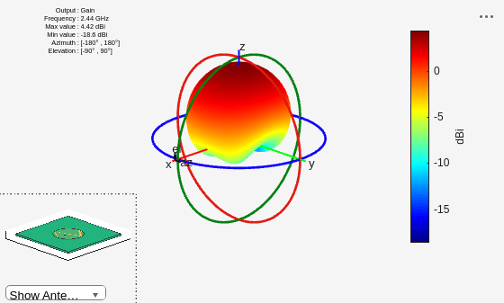
% Operating frequency
f = 2.44e9;

% Geometry
gnd = 80e-3;
h = 1.53e-3;
r = 16.8e-3;
feedloc = [5.1e-3 0];

% RF Connector dimensions
DinFeed = 1.25e-3;
DoutFeed = 4.1e-3;

% FR4 substrate
d = dielectric(Name='FR4',EpsilonR=4.3,LossTangent=0.015,Thickness=h);
Create a circular patch antenna based on these parameters.
patch = patchMicrostripCircular(GroundPlaneLength=gnd,GroundPlaneWidth=gnd,...
    Radius=r,Height=h,Substrate=d,FeedOffset=feedloc);
Convert the circular patch antenna into a PCB stack and define the feed parameters.
p = pcbStack(patch);
p.FeedViaModel = 'square';
p.FeedDiameter = DinFeed;
Refine the mesh of this antenna. Define an RF connector for this PCB stack. Compute and plot radiation pattern using the FEM solver.
[~] = mesh(p,MaxEdgeLength=0.0035);
p.SolverType = 'FEM';
connector = RFConnector(InnerRadius=0.5*DinFeed,OuterRadius=0.5*DoutFeed,...
    EpsilonR=2,PinLength=0);
p.Connector = connector;
pattern(p,f)
Supported Catalog Elements
The following antennas and arrays from the catalog can be converted into a PCB antenna
by the pcbStack object:
Antennas
Note
Orient these antennas in the xy-plane if required,
before conversion to pcbStack.
Dipole Antennas:
dipole,bowtieTriangular,bowtieRounded, anddipoleBlade.Fractal Antennas:
fractalCarpet,fractalGasket,fractalIsland,fractalKoch,fractalSnowflakeLoop Antennas:
loopCircular,loopRectangularMonopole Antennas:
invertedFcoplanar,invertedLcoplanarPatch Antennas:
patchMicrostrip,patchMicrostripCircular,patchMicrostripElliptical,patchMicrostripEnotch,patchMicrostripHnotch,patchMicrostripInsetfed,patchMicrostripTriangularReflector Antennas:
reflectorandreflectorCircularwith a finite ground plane.Slot Antennas:
slot,vivaldi,vivaldiAntipodal,vivaldiOffsetCavitySpiral Antennas:
spiralArchimedean,spiralEquiangular,spiralRectangularOther Antennas:
lpda,customAntennaGeometry,customArrayGeometry
Arrays
Note
The arrays must be homogeneous, with uniform elements.
linearArraycircularArrayrectangularArray
References
[1] Balanis, C. A. Antenna Theory. Analysis and Design. 3rd Ed. Hoboken, NJ: John Wiley & Sons, 2005.
[2] Stutzman, W. L. and Gary A. Thiele. Antenna Theory and Design. 3rd Ed. River Street, NJ: John Wiley & Sons, 2013.